|
Intel Corporation is an American multinational semiconductor chip maker corporation headquartered in Santa Clara, California. Intel is the world's largest and highest valued semiconductor chip maker, based on revenue. It is the inventor of the x86 series of microprocessors, the processors found in most personal computers. Intel Corporation, founded on July 18, 1968, is a portmanteau of Integrated Electronics (the fact that "intel" is the term for intelligence information was also quite suitable). Intel also makes motherboard chipsets, network interface controllers and integrated circuits, flash memory, graphic chips, embedded processors and other devices related to communications and computing. Founded by semiconductor pioneers Robert Noyce and Gordon Moore and widely associated with the executive leadership and vision of Andrew Grove, Intel combines advanced chip design capability with a leading-edge manufacturing capability. Though Intel was originally known primarily to engineers and technologists, its "Intel Inside" advertising campaign of the 1990s made it and its Pentium processor household names.
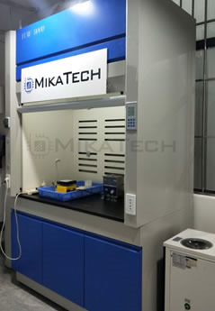
- Mikatech Intel MCU reverse engineer list:
-
 87xx series mcu code extraction: 8741 8741AH 8742 8742AH 8744 8744H 8748 8748H 8749 8749H 8751 8751BH 8751H 8751H-8 87551SB 8752BH 8796BH 8796JF 8797BH 8797JF 8798 ... 87xx series mcu code extraction: 8741 8741AH 8742 8742AH 8744 8744H 8748 8748H 8749 8749H 8751 8751BH 8751H 8751H-8 87551SB 8752BH 8796BH 8796JF 8797BH 8797JF 8798 ...
87Cxx series mcu code extraction: 87C151SA 87C151SB 87C194 87C196CA 87C196JQ 87C196JR 87C196JT 87C196JV 87C196KB 87C196KC 87C196KD 87C196KQ 87C196KR 87C196KS 87C196KT 87C196LA 87C196MC 87C196MH 87C198 87C251SA 87C251SB 87C251SP 87C251SQ 87C42 87C51 87C51FA 87C51FB 87C51FC 87C51GB 87C51RA 87C51RB 87C51RC 87C52 87C54 87C58 D87C51 D87C151SA D87C151SB D87C194 D87C198 D87C251SA D87C251SP D87C251SQ D87C196CA D87C42 D87C51FA D87C51FB D87C51FC D87C251SB D87C51RA D87C196JQ D87C196JR D87C196JT D87C196JV D87C196KR D87C196KS D87C196KT D87C196LA D87C51RB D87C51RC D87C52 D87C54 D87C51GB D87C58 D87L42 D87L51FA D87L51FB D8751BH D87L51FC D87L52 D87L54 8749 D87L58 D8741 D8741AH D8742 DD8749H D8742AH D8744 D8744H D8748 D8751 8D748H D8751H D8751H-8 D8752BH D8798 D8796BH D8796JF D8797BH D8797JF D87C196MC D87C196MH D87C251SA...
87Lxx series Microprocessor code retreive: 87L42 87L51FA 87L51FB 87L51FC 87L52 87L54 87L58 ...
D87Cxx series mcu code extraction: D87C51 D87C52 D87C54 D87C58 D87C51FA D87C51FB D87C51FC D87C196KC D87C196MC D87C196MD D87C196MH D89C196MD...
Intel MCS-51
The Intel MCS-51 (commonly referred to as 8051) is a Harvard architecture, CISC instruction set, single chip microcontroller (µC) series which was developed by Intel in 1980 for use in embedded systems. Intel's original versions were popular in the 1980s and early 1990s and enhanced binary compatible derivatives remain popular today.
Intel's original MCS-51 family was developed using NMOS technology, but later versions, identified by a letter C in their name (e.g., 80C51) used CMOS technology and consume less power than their NMOS predecessors. This made them more suitable for battery-powered devices.
The family was in 1996 continued with the enhanced 8-bit MCS-151 and the 8/16/32-bit MCS-251 family of binary compatible microcontrollers.[2] While Intel no longer manufactures the MCS-51, MCS-151 and MCS-251 family, enhanced binary compatible derivatives made by numerous vendors remain popular today. Some derivatives integrate a digital signal processor (DSP). In addition to these physical devices, several companies also offer MCS-51 derivatives as IP cores for use in FPGAs or ASICs designs.
i8051 microarchitecture.
The 8051 architecture provides many functions (CPU, RAM, ROM, I/O, interrupt logic, timer, etc.) in a single package
8-bit ALU and Accumulator, 8-bit Registers (one 16-bit register with special move instructions), 8-bit data bus and 2x16-bit address bus/program counter/data pointer and related 8/11/16-bit operations; hence it is mainly an 8-bit microcontroller
Boolean processor with 17 instructions, 1-bit accumulator, dump retrieve 32 registers (4 bit addressable 8-bit) and up to 144 special 1-bit addressable RAM variables (18 bit addressable 8-bit)
Multiply, divide and compare instructions
4 fast switchable register banks with 8 registers each (memory mapped)
Fast interrupt with optional register bank switching
Interrupts and threads with selectable priority
Dual 16-bit address bus – It can access 2 x 216 memory locations – 64 kB (65536 locations) each of RAM and ROM
128 bytes of on-chip RAM (IRAM)
4 KiB of on-chip ROM, with a 16-bit (64 KiB) address space (PMEM). Not included on 803X variants
Four 8-bit bi-directional input/output port
UART (serial port)
Two 16-bit Counter/timers
Power saving mode (on some derivatives)
One particularly usefulfeature of the 8051 core is the inclusion of a boolean processing engine which allows bit-level boolean logic operations to be carried out directly and efficiently on select internal registers and select RAM locations. This advantageous feature helped cement the 8051's popularity in industrial control applications because it reduced code size by as much as 30%.[citation needed] Another valued[citation needed] feature is the inclusion of four bank selectable working read protected HEX
data code fuses
unlock blocked
protect erase register sets which greatly reduce the amount of time required to complete an interrupt service routine. With a single instruction the 8051 can switch register banks as opposed to the time consuming task of transferring the critical registers to the stack or designated RAM locations. These registers also allowed the 8051 to quickly perform a context switch.
The MCS-51 UARTs make it simple to use the chip as a serial communications interface. External pins can be configured to connect to internal shift registers in a variety of ways, and the internal timers can also be used, allowing serial communications in a number of modes, both synchronous and asynchronous. Some modes allow communications with no external decapsulation and code recovery
copy contents of crypto memory
read EEprom and ROM
flash memory get read components. A mode compatible with an RS-485 multi-point communications environment is achievable, but the 8051's real strength[editorializing] is fitting in with existing ad-hoc protocols (e.g., when controlling serial-controlled devices).
Once a UART, and a timer if necessary, have been configured, the programmer needs only to write a simple interrupt routine to refill the send shift register whenever the last bit is shifted out by the UART and/or empty the full receive shift register (copy the data somewhere else). The main program then performs serial reads and writes simply by reading and writing 8-bit data to stacks.
MCS-51 based microcontrollers typically include one or two UARTs, two or three timers, 128 or 256 bytes of internal data RAM (16 bytes of which are bit-addressable), up to 128 bytes of I/O, 512 bytes to 64 kB of internal disassemble file
recovering protected code
unprotect
remove the protection fuses
read-out of an EEPROM processor
dump flash and eeprom program memory, and sometimes a quantity of extended data RAM (ERAM) located in the external data space. The original 8051 core ran at 12 clock cycles per machine cycle, with most instructions executing in one or two machine cycles. With a 12 MHz clock frequency, the 8051 could thus execute 1 million one-cycle instructions per second or 500,000 two-cycle instructions per second. Enhanced 8051 cores are now commonly used which run at six, four, two, or even one clock per machine cycle, and have clock frequencies of up to 100 MHz, and are thus capable of an even greater number of instructions per second. All SILabs, some Dallas and a few Atmel devices have single cycle cores.
8051 variants include built-in reset timers with brown-out detection, on-chip oscillators, self-programmable Flash ROM program memory, built-in external RAM, extra internal program storage, bootloader code in ROM, EEPROM non-volatile data storage, I²C, SPI, and USB host interfaces, CAN or LIN bus, PWM generators, analog comparators, A/D and D/A converters, RTCs, extra counters and timers, in-circuit debugging facilities, more interrupt sources, and extra power saving modes.
In many engineering schools the 8051 microcontroller is used in introductory microcontroller courses.
Memory architecture
The MCS-51 has four distinct types of memory – internal RAM, special function registers, program memory, and external data memory.
Internal RAM (IRAM) is located from address 0 to address 0xFF. IRAM from 0x00 to 0x7F can be accessed directly. IRAM from 0x80 to 0xFF must be accessed indirectly, using the @R0 or @R1 syntax, with the address to access loaded in R0 or R1. The 128 bits at IRAM locations 0x20–0x2F are bit-addressable.
Special function registers (SFR) are located in the same address space as IRAM, at addresses 0x80 to 0xFF, and are accessed directly using the same instructions as for the lower half of IRAM. They can not be accessed indirectly via @R0 or @R1. 16 of the SFRs are also bit-addressable.
Program memory (PMEM, though less common in usage than IRAM and XRAM) is up to 64 KiB of read-only memory, starting at address 0 in a separate address space. It may be on- or off-chip, depending on the particular model of chip being used. Program memory is read-only, though some variants of the 8051 use on-chip flash memory and provide a method of re-programming the memory in-system or in-application. In addition to code, it is possible to store read-only data in program memory, accessed by the MOVC A, @DPTR instruction. Data is fetched from the address specified in the 16-bit special function register DPTR.
External data memory (XRAM) is a third address space, also starting at address 0. It can also be on- or off-chip; what makes it "internal" is that it must be accessed using the MOVX (Move eXternal) instruction. Many variants of the 8051 include the standard 256 bytes of IRAM plus a few kB of XRAM on the chip.
The 8051 is designed as a strict Harvard architecture. The 8051 can only execute code fetched from program memory. The 8051 does not have any instruction to write to program memory. Most 8051 systems respect this distinction, and so are unable to download and directly execute new programs. The strict Harvard architecture has the advantage of making such recovery read data
break password
retrieving hex source code
source code blocked
lockbits activated
read security bytes systems immune to most forms of malware. Some 8051 systems have (or can be modified to have) some "dual-mapped" RAM, making them act somewhat more like Princeton architecture. This (partial) Princeton architecture has the advantage of making it possible for a Forth boot loader running on the 8051 to write new native code to RAM and then execute it, leading to faster incremental and interactive programming cycles than strict Harvard systems.
Registers
The only register on an 8051 that is not memory-mapped is the 16-bit program counter PC. This specifies the address of the next instruction to execute. Relative branch instructions supply an 8-bit signed offset which is added to the PC.
The following registers are memory-mapped into the special function register space:
(0x81) Stack pointer SP. This is an 8-bit register used by subroutine call and return instructions. The stack grows upward; the SP is incremented before pushing, and decremented after popping a value.
(0x82–83) Data pointer DP. This is a 16-bit register that is used for accessing PMEM and XRAM.
(0xD0) Program status word PSW. This contains important status flags:
PSW.0: P Parity. Gives the parity (modulo-2 sum of the bits of) the most recent ALU result.
PSW.1: UD User Defined. For general software use, not otherwise used by hardware.
PSW.2: OV Overflow flag. Set when addition produces a signed overflow.
PSW.3: RS0 Register select 0. The low-order bit of the register bank snaileye. Set when banks at 0x08 or 0x18 are in use.
PSW.4: RS1 Register select 1. The high-order bit of the register bank. Set when banks at 0x10 or 0x18 are in use.
PSW.5: F0 Flag 0. For general software use, not otherwise used by hardware.
PSW.6: AC auxiliary carry. Set when addition produces a carry from bit 3 to bit 4.
PSW.7: C Carry bit.
(0xE0) Accumulator A. This register is used by most instructions.
(0xF0) B register. This is used as an extension to the accumulator for multiply and divide instructions.
In addition, there are 8 general purpose registers R0–R7, mapped to IRAM between 0x00 and 0x1F. Only 8 bytes of that range are used at any given time, determined by the bank select bits in the PSW.
256 single bits are directly addressable. These are the 16 IRAM locations from 0x20–0x2F, and the 16 special function registers 0x80, 0x88, 0x90, …, 0xF8.
Note that the PSW does not contain the common N (negative) and Z (zero) flags. Instead, because the accumulator is a bit-addressible SFR, it is possible to branch on individual bits of it, including the msbit. There is also an instruction to jump if the accumulator is zero or non-zero.
Instruction set
Instructions are all 1 to 3 bytes long, consisting of an initial opcode byte, followed by up to 2 bytes of operands.
There are 16 basic ALU instructions that operate between the accumulator and a second operand, specified using one of the following addressing modes:
Register direct, R0–R7 (opcodes x8–xF)
Register indirect, @R0 or @R1 (opcodes x6 and x7)
Memory direct, specifying an IRAM or SFR location (opcodes x5, followed by 1 byte of address)
Immediate, specifying an 8-bit constant (opcodes x4, followed by 1 byte of data)
The instructions are as follows. Not all support all addressing modes; the immediate mode in particular is sometimes nonsensical:
0y INC operand: Increment the specified operand. Opcode 04 specifies "INC A"
1y DEC operand: Decrement the specified operand. Opcode 14 specifies "DEC A"
2y ADD A,operand: Add the operand to the accumulator A.
3y ADDC A,operand: Add the operand, plus the C bit, to the accumulator.
4y ORL A,operand: Logical OR the operand into the A register.
5y ANL A,operand: Logical AND the operand into the A register.
6y XRL A,operand: Logical exclusive-OR the operand into the A register.
7y MOV operand,#data: Move immediate data to the operand. Opcode 74 specifies "MOV A,#data.
8y MOV address,operand: Move data to an IRAM or SFR register.
9y SUBB A,operand: Subtract the operand from the accumulator, with borrow. Note there is no subtract without borrow.
Ay MOV operand,address: Move data from an IRAM or SFR register. Opcodes A4 and A5 are not used.
By CJNE operand,#data,offset: Compare operand to the recover code from encrypted
hacking hex file
readback protected
read eeprom data
break protect code
copy an encrypted IC immediate data, and branch to PC+address if not equal. Opcodes B4 and B5 perform CJNE A,operand,offset, for memory direct and immediate operands. Note there is no "compare and jump if equal" instruction.
Cy XCH A,operand: Exchange (swap) the accumulator and the operand. Opcode C4 is not used.
Dy DJNZ operand,offset: Decrement the operand, and branch to PC+offset if the result is non-zero. Opcodes D4, D6, and D7 are not used.
Ey MOV A,operand: Move operand to the accumulator. Opcode E4 is not used. (Use opcode 74 instead.)
Fy MOV operand,A: Move accumulator to the operand. Opcode F4 is not used.
Only the ADD, ADDC and SUBB instructions set PSW flags. The INC, DEC, and logical instructions do not. The CJNE instructions modify the C bit only, to the borrow that results from operand1−operand2.
The 32 opcodes 0x00–0x3F, plus the few opcodes not used in the above range, are used for other instructions with more limited operand-specification capabilities.
One of the reasons for the 8051's popularity is its range of operations on single bits. Bits are always specified by absolute addresses; there is no register-indirect or indexed addressing. Instructions that operate on single bits are:
SETB bit, CLR bit, CPL bit: Set, clear, or complement the specified bit
JB bit,offset: Jump if bit set
JNB bit,offset: Jump if bit clear
JBC bit,offset: Jump if bit set, and clear bit
MOV C,bit, MOV bit,C: Move the specified bit to the carry bit, or vice-versa
ORL C,bit, ORL C,/bit: OR the bit (or its complement) to the carry bit
ANL C,bit, ANL C,/bit: AND the bit (or its complement) to the carry bit
XRL C,bit, XRL C,/bit: Exclusive-OR the bit (or its complement) to the carry bit
Although most instructions require that one operand is the accumulator or an immediate constant, it is possible to perform a MOV directly between two internal RAM locations.
Programming
Main article: 8051 compiler
There are various high-level programming language compilers for the 8051. Several C compilers are available for the 8051, most of which allow the programmer to specify where each variable should be stored in its six types of memory, and provide access to 8051 specific hardware features such as the multiple register banks and bit read out memory
Read Data from EEprom
extract software
decrypting memory dump manipulation instructions. There are many commercial C compilers. SDCC is a popular[citation needed] open source C compiler. Other high level languages such as C++, Forth, BASIC, Pascal/Object Pascal, PL/M and Modula-2 are available for the 8051, but they are less widely used[citation needed] than C and assembly.
Because IRAM, XRAM, and PMEM (read only) all have an address 0, C compilers for the 8051 architecture provide compiler-specific pragmas or other extensions to indicate where a particular piece of data should be stored (i.e. constants in PMEM or variables needing fast access in IRAM). Since data could be in one of three memory spaces, a mechanism is usually provided to allow determining to which memory a pointer refers, either by constraining the pointer type to include the memory space, or by storing metadata with the pointer.
Related processors
Intel 8031 processors
The 8051's predecessor, the 8048, was used in the keyboard of the first IBM PC, where it converted keypresses into the serial data stream which is sent to the main unit of the computer. The 8048 and derivatives are still used today for basic model keyboards.
The 8031 was a cut down version of the original Intel 8051 that did not contain any internal program memory (ROM). To use this chip, external ROM had to be added containing the program that the 8031 would fetch and execute. An 8051 chip could be sold as a ROM-less 8031, as the 8051's internal ROM is disabled by the normal state of the EA pin in an 8031-based design. A vendor might sell an 8051 as an 8031 for any number of reasons, such as faulty code in the 8051's ROM, or simply an oversupply of 8051's and undersupply of 8031's.
The 8052 was an enhanced version of the original 8051 that featured 256 bytes of internal RAM instead of 128 bytes, 8 kB of ROM instead of 4 kB, and a third 16-bit timer. The 8032 had these same features except for the internal ROM program memory. Most modern "8051-compatible" microcontrollers include these features.
Intel discontinued its MCS-51 product line in March 2007,[7] however there are plenty of enhanced 8051 products or silicon intellectual property added regularly from other vendors. Current vendors of MCS-51 compatible processors include more than 20 independent code read Microprocessor
extract code
read Memory
copy eeproms
get bin code
read program
get firmware manufacturers including Atmel, Infineon Technologies (formerly Siemens AG), Maxim Integrated Products (via its Dallas Semiconductor subsidiary), NXP (formerly Philips Semiconductor), Microchip Technology, Nuvoton (formerly Winbond), ST Microelectronics, Silicon Laboratories (formerly Cygnal), Texas Instruments, Ramtron International, Silicon Storage Technology, Cypress Semiconductor and Analog Devices.
The 80C537 and 80C517 are CMOS versions, designed for the automotive industry. Enhancements mostly include new peripheral features and expanded arithmetic instructions. The 80C517 has fail-safe mechanisms, analog signal processing facilities and timer capabilities and 8 kB on-chip program memory. Other features include:
256 byte on-chip RAM
256 directly addressable bits
External program and data memory expandable up to 64 kB
8-bit A/D converter with 12 multiplexed inputs
Arithmetic unit can make division, multiplication, shift and normalize operations
Eight data pointers instead of one for indirect addressing of program and external data memory
Extended watchdog facilities
Nine ports
Two full-duplex serial interfaces with own baud rate generators
Four priority level interrupt systems, 14 interrupt vectors
Three power saving modes
Use as intellectual property
Today, 8051s are still available as discrete parts, but they are mostly used as silicon intellectual property cores.[citation needed] Available in high-level language source code (VHDL or Verilog) or FPGA netlist forms, these cores are typically integrated within embedded systems, in products ranging from USB flash drives to washing machines to complex open a locked Microcontroller
mcu lockbit lock
duplicate controller
obtain source code wireless communication systems on a chip. Designers use 8051 silicon IP cores, because of the smaller size, and lower power, compared to 32 bit processors like ARM M series, MIPS and BA22. Modern 8051 cores are faster than earlier packaged versions. Design improvements have increased 8051 performance while retaining compatibility with the original MCS 51 instruction set. The original Intel 8051 ran at 12 clock cycles per machine cycle, and most instructions executed in one or two machine cycles. A typical maximum clock frequency of 12 MHz meant these old 8051s could execute one million single-cycle instructions, or 500,000 two-cycle instructions, per second. In contrast, enhanced 8051 silicon IP cores now run at one clock cycle per machine cycle, and have clock frequencies of up to 450 MHz. FIB聚焦离子束线路修改 That means an 8051-compatible processor can now execute 450 million instructions per second.
MCU based on 8051
Atmel: AT89C51, AT89S51, AT83C5134
NXP: NXP700 and NXP900 series
Infineon: XC800
Digital signal processor (DSP) variants
Several variants with an additional 16-bit digital signal processor (DSP) (for example for MP3 or OGG coding/decoding) with up to 675 million instructions per second (maker MIPS)[9] and integrated USB 2.0 interface[10] or as intellectual property[11] exist.
Enhanced 8-bit binary compatible microcontroller: MCS-151 family
This section requires expansion. (May 2013)
1996 Intel announced the MCS-151 family, an up to 6 times faster variant.[2] 8051 fully binary and instruction set compatible, but with pipelined CPU, 16 bit internal code bus and 6x speed. The MCS-151 family was also discontinued by Intel, but is widely available in binary compatible and partly enhanced variants.
8/16/32-bit binary compatible microcontroller: MCS-251 family
This section requires expansion. (May 2013)
The 80251 8/16/32-bit microcontroller with 16MB (24-bit) address-space and 6 times faster instruction cycle was introduced by Intel in 1996.[2][12] It can perform as an 8-bit 8051, has 24-bit get hex code
source code recovery
extract encryption
source code retreive
security external address space which is 16-bit wide segmented and 32-bit ALU with mostly 8/16/32-bit wide data instructions silicon wafer Focused Ion Beam processing (also Boolean processor with special registers/memory) and a large CISC instruction set, 40 8/16/32-bit registers with 8 8-bit registers in 4 times fast switching memory banks (maximum 512 addressable 8-bit special registers).
It features extended instructions - see also the programmer's guide - and later variants with higher performance, also available as intellectual property (IP). It is 3-stage pipelined. The MCS-251 family was also discontinued by Intel, but is widely available in binary compatible and partly enhanced variants from many manufacturers
|