|
Xilinx, Inc. is an American technology company, primarily a supplier of programmable logic devices. It is known for inventing the field programmable gate array (FPGA) and as the first semiconductor company with a fabless manufacturing model.
Founded in Silicon Valley in 1984, the company is headquartered in San Jose, California, with additional offices in Longmont, Colorado; Dublin, Ireland; Singapore; Hyderabad, India; Beijing, China; Shanghai, China and Tokyo, Japan.
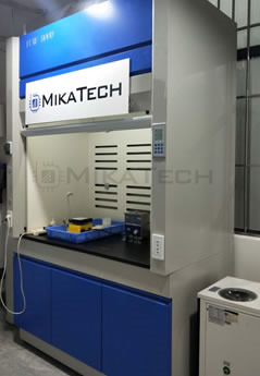
- Mikatech Xilinx MCU reverse engineer list:
History
Early days
Ross Freeman, Bernard Vonderschmitt, and James V Barnett II, who all had worked for integrated circuit and solid-state device manufacturer Zilog Corp, founded Xilinx in 1984.
While working for Zilog, Freeman wanted to create chips that acted like a blank tape, allowing users to program the technology themselves. At the time, the concept was paradigm-changing.[6] "The concept required lots of transistors and, at that time, transistors were considered extremely precious – people thought that Ross's idea was pretty far out", said Xilinx Fellow Bill Carter, who when hired in 1984 as the first IC designer was the Xilinx's eighth employee.
Big semiconductor manufacturers were enjoying strong profits by producing massive volumes of generic circuits.[4] Designing and manufacturing dozens of different circuits for specific markets offered lower profit margins and required greater manufacturing complexity.[4] What became known as the FPGA would allow circuits produced in quantity to be tailored by individual market segments.
Freeman failed to convince Zilog to invest in creating the FPGA to chase what was only a $100 million market at the time.[4] Freeman and Barnett left Zilog and teamed up with their 60-year-old ex-colleague Bernard Vonderschmitt to raise $4.5 million in venture funding to design the first commercially-viable FPGA.[4] They incorporated the company in 1984 and began selling its first product by 1985.
By late 1987 the company had raised more than $18 million in venture capital (worth approximately $36 million in 2013 dollars adjusted for inflation) and generated revenues at an annualized rate of nearly $14 million.
Growth
As demand for programmable logic continued to grow, so did Xilinx's revenues and profits.[4]
From 1988 to 1990, the company's revenue grew each year from $30 million to $50 million to $100 million.[4] During this time period, the company which had been providing funding to Xilinx, Monolithic Memories Inc. (MMI), was purchased by Xilinx competitor AMD.[4] As a result, Xilinx dissolved the deal with MMI and went public on the NASDAQ in 1989.[4] The company also moved to a 144,000-square-foot (13,400 m2) plant in San Jose, California in order to keep pace with demand from companies like HP, Apple Inc., IBM and Sun Microsystems who were buying large quantities from Xilinx.
Xilinx competitors emerged in the FPGA market in the mid-1990s.[4] Despite the competition, Xilinx’s sales grew to $135 million in 1991, $178 million in 1992 and $250 million in 1993.
The company reached $550 million in revenue in 1995, one decade after having sold its first product.
According to market research firm iSuppli, Xilinx has held the lead in programmable logic device market share since the late 1990s. Over the years, Xilinx expanded operations to India, Asia and Europe.
Xilinx's sales rose from $560 million in 1996 to $2.2 billion by the end of its fiscal year 2013.[12][13] Moshe Gavrielov – an EDA and ASIC industry veteran who was appointed as president and CEO in early 2008 – introduced targeted design platforms to provide solutions that combine FPGAs with software, IP cores, boards and kits to address focused target applications.[14] These targeted design platforms are an alternative to costly application-specific integrated circuits (ASICs) and application-specific standard products (ASSPs).
Today
The company has expanded its product portfolio since its founding. Xilinx sells a broad range of FPGAs, complex programmable logic devices (CPLDs), design tools, intellectual property and reference designs.[1] Xilinx also has a global services and training program.[1]
After using the introduction of 3D chips to deliver more powerful FPGAs, Xilinx then adapted the technology to combine formerly separate components in a single chip, first combining an FPGA with transceivers to boost bandwidth capacity while using less power.[18] According to Xilinx CEO Moshe Gavrielov, the addition of a heterogeneous communications device, combined with the introduction of new software tools and the Zynq-7000 line of 28 nm SoC devices that combine an ARM core with an FPGA, are part of shifting its position from a programmable logic device supplier to one delivering “all things programmable”.
The company's products have been recognized by EE Times, EDN and others for innovation and market impact.
In addition to Zynq-7000, Xilinx product lines (see Current Family Lines) include the Virtex, Kintex and Artix series, each including configurations and models optimized for different applications.[23] With the introduction of the Xilinx 7 series in June, 2010, the company has moved to three major focused ion beam laboratory service FPGA product families, the high-end Virtex, the mid-range Kintex family and the low-cost Artix family, retiring the Spartan brand, which ends with the Xilinx Series 6 FPGAs. In April 2012, the company introduced the Vivado Design Suite - a next-generation SoC-strength design environment for advanced electronic system designs.
Technology
The Spartan-3 platform was the industry’s first 90nm FPGA, delivering more functionality and bandwidth per dollar than was previously possible, setting new standards in the programmable logic industry.
Xilinx designs, develops and markets programmable logic products, including integrated circuits (ICs), software design tools, predefined system functions delivered as intellectual property (IP) cores, design services, customer training, field engineering and technical support.[1] Xilinx sells both FPGAs and CPLDs for electronic equipment manufacturers in end markets such as communications, industrial, consumer, automotive and data processing.
Xilinx's FPGAs have been used for the ALICE (A Large Ion Collider Experiment) at the CERN European laboratory on the French-Swiss border to map and disentangle the trajectories of thousands of subatomic particles.[34] Xilinx has also engaged in a partnership with the United States Air Force Research Laboratory’s Space Vehicles Directorate to develop FPGAs to withstand the damaging effects of radiation in space, which are 1,000 times less sensitive to space radiation than the commercial equivalent, for deployment in new satellites.[35]
The Virtex-II Pro, Virtex-4, Virtex-5, and Virtex-6 FPGA families, which include up to two embedded IBM PowerPC cores, are targeted to the needs of system-on-chip (SoC) designers.
Xilinx FPGAs can run a regular embedded OS (such as Linux or vxWorks) and can implement processor peripherals in programmable logic.
Xilinx's IP cores include IP for simple functions (BCD encoders, counters, etc.), for domain specific cores (digital signal processing, FFT and FIR cores) to complex systems (multi-gigabit networking cores, the MicroBlaze soft microprocessor and the compact Picoblaze
microcontroller).[1] Xilinx also creates custom cores for a fee.
The main design toolkit Xilinx provides engineers is the Vivado Design Suite, and integrated design environment (IDE) with a system-to-IC level tools built on a shared scalable data model and a common debug environment. Vivado includes electronic system level (ESL) design tools for synthesizing and verifying C-based algorithmic IP; standards based packaging open a locked Microcontroller
mcu lockbit lock
read-out of an EEPROM processor
dump flash and eeprom of both algorithmic and RTL IP for reuse; standards based IP stitching and systems integration of all types of system building blocks; and the verification of blocks and systems.[39] A free version WebPACK Edition of Vivado provides designers with a limited version of the design environment.
Xilinx's Embedded Developer's Kit (EDK) supports the embedded PowerPC 405 and 440 cores (in Virtex-II Pro and some Virtex-4 and -5 chips) and the Microblaze core. Xilinx's System Generator for DSP implements DSP designs on Xilinx FPGAs. A freeware version of its EDA software decapsulation and code recovery
copy contents of crypto memory
disassemble file called ISE WebPACK is used with some of its non-high-performance chips. Xilinx is the only (as of 2007) FPGA vendor to distribute a native Linux freeware synthesis toolchain.
Xilinx announced the architecture for a new ARM Cortex A9-based platform for embedded systems designers, that combines the software programmability of an embedded processor with the hardware flexibility of an FPGA. The new architecture abstracts much of the hardware burden away from the embedded software developers' point of view, giving them an unprecedented level of control in the development process.With this platform, software developers can leverage their existing system code based on ARM technology and utilize vast off-the-shelf open-source recovering protected code
unprotect
remove the protection fuses
read Memory
copy eeproms and commercially available software component libraries.Because the system boots an OS at reset, software development can get under way quickly within familiar development and debug environments using tools such as ARM’s RealView development suite and related third-party tools, Eclipse-based IDEs, GNU, the Xilinx Software Development Kit and others.
In early 2011, Xilinx began shipping a new device family based on this architecture. The Zynq-7000 SoC platform immerses ARM multi-cores, programmable logic fabric, DSP data paths, memories and I/O functions in a dense and configurable mesh of interconnect.[46][47] The platform targets get bin code
read program
get firmware
recovery read data
read rom embedded designers working on market applications that require multi-functionality and real-time responsiveness, such as automotive driver assistance, intelligent video surveillance, industrial automation, aerospace and defense, and next-generation wireless.
Following the introduction of its 28 nm 7-series FPGAs, Xilinx revealed that that several of the highest-density parts in those FPGA product lines will be constructed using multiple dice in one package, employing technology developed for 3D construction and stacked-die assemblies. The company’s duplicate controller
obtain source code
code read Microprocessor
extract code stacked silicon interconnect (SSI) technology stacks several (three or four) active FPGA dice side-by-side on a silicon interposer – a single piece of silicon that carries passive interconnect. The individual FPGA dice are conventional, and are flip-chip mounted by microbumps on to the interposer. The interposer provides direct interconnect between the FPGA dice, with no need for transceiver technologies such as high-speed SERDES.[48][49][50] In October 2011, Xilinx shipped the first FPGA to use the new technology, the Virtex-7 2000T FPGA, which includes 6.8 billion transistors and 20 million ASIC gates. The following spring, Xilinx used the 3D technology to ship the Virtex-7 HT, the industry’s first read security bytes
break password
retrieving hex source code heterogeneous FPGAs, which combine high bandwidth FPGAs with up to sixteen 28 Gbit/s and seventy-two 13.1 Gbit/s transceivers to reduce power and size requirements for key Nx100G and 400G line card applications and functions.
In January 2011, Xilinx acquired design tool firm AutoESL Design Technologies and added System C high-level design for its 6- and 7-series FPGA families.[57] The addition of AutoESL tools extends the design community for FPGAs to designers more accustomed to designing at a higher level of abstraction using C, C++ and System C.
In April 2012, Xilinx introduced a redesign of its toolset for programmable systems, called Vivado Design Suite. This IP and system-centric design software supports newer high capacity devices, and speeds the design of programmable logic and I/O.[59] Vivado provides source code blocked
break protect code
copy an encrypted IC faster integration and implementation for programmable systems into devices with 3D stacked silicon interconnect technology, ARM processing systems, analog mixed signal (AMS), and many semiconductor intellectual property (IP) cores.
Current family lines
Prior to 2010, Xilinx offered two main FPGA families: the high-performance Virtex series and the high-volume Spartan series, with a cheaper EasyPath option for ramping to volume production.[23] The company also provides two CPLD lines: the CoolRunner and the 9500 series. Each extract software
decrypting memory dump
recover code from encrypted model series has been released in multiple generations since its launch.[61] With the introduction of its 28 nm FPGAs in June 2010, Xilinx replaced the high-volume Spartan family with the Kintex family and the low-cost Artix family.
In newer FPGA products, Xilinx minimizes total power consumption by the adoption of a high-K metal gate (HKMG) process, which allows for low static power consumption. At the 28 nm node, static power is a significant portion of the total power dissipation of a device and in some cases is the dominant factor. Through the use of a HKMG process, Xilinx has reduced power use while hacking hex file
lockbits activated
read out memory increasing logic capacity.[62] Virtex-6 and Spartan-6 FPGA families are said to consume 50 percent less power, and have up to twice the logic capacity compared to the previous generation of Xilinx FPGAs.
In June, 2010 Xilinx introduced the Xilinx 7 series: the Virtex-7, Kintex-7, and Artix-7 families, promising improvements in system power, performance, capacity, and price. These new FPGA families are manufactured using TSMC's 28 nm HKMG process.[65] The 28 nm series 7 devices feature a 50 percent power reduction compared to the company's 40 nm devices Read Data from EEprom
readback protected
read eeprom data and offer capacity of up to 2 million logic cells.Less than one year after announcing the 7 series 28 nm FPGAs, Xilinx shipped the world’s first 28 nm FPGA device, the Kintex-7, making this the programmable industry’s fastest product rollout. In March 2011, Xilinx introduced the Zynq-7000 family, which integrates a complete ARM Cortex-A9 MPCore processor-based system on a 28 nm FPGA for system architects and embedded software developers.
Virtex family
The Virtex series of FPGAs have integrated features that include FIFO and ECC logic, DSP blocks, PCI-Express controllers, Ethernet MAC blocks, and high-speed transceivers. In addition to FPGA logic, the Virtex series includes embedded fixed function hardware for commonly used functions such as multipliers, memories, serial transceivers and microprocessor cores.[68] These capabilities are used in applications such as wired and wireless infrastructure equipment, advanced medical equipment, test and measurement, and defense systems.[69] Some Virtex family members are available in get hex code
source code recovery
flash memory
protect erase radiation-hardened packages, specifically to operate in space where harmful streams of high-energy particles can play havoc with semiconductors. The Virtex-5QV FPGA was designed to be 100 times more resistant to radiation than previous radiation-resistant models and offers a ten-fold increase in performance. However, characterization and test data were not yet available for the Virtex-5QX on the Xilinx Radiation Test Consortium website as of November 2011.
Xilinx's most recently announced Virtex, the Virtex 7 family, is based on a 28 nm design and is reported to deliver a two-fold system performance improvement at 50 percent lower power compared to previous generation Virtex-6 devices. In addition, Virtex-7 doubles the memory bandwidth compared to previous generation Virtex FPGAs with 1866 Mbit/s memory interfacing performance and over two million logic cells.
In 2011, Xilinx began shipping sample quantities of the Virtex-7 2000T FPGA, which combines four smaller FPGAs into a single package by placing them on a special silicon interconnection pad (called an interposer) to deliver 6.8 billion transistors in a single large chip. The interposer provides 10,000 data pathways between the individual FPGAs – roughly 10 to 100 times more than would extract encryption
source code retreive
security
read protected HEX usually be available on a board – to create a single FPGA. In 2012, using the same 3D technology, Xilinx introduced initial shipments of their Virtex-7 H580T FPGA, a heterogeneous device, so called because it comprises two FPGA dice and one 8-channel 28Gbit/s transceiver die in the same package.
As Xilinx introduced new high capacity 3D FPGAs, including Virtex-7 2000T and Virtex-7 H580T products, these devices began to outpace the capacity of Xilinx’s design software, which led the company to completely redesign its tool set. The result was the introduction maker together club of data code fuses
unlock blocked
open a locked Microcontroller
mcu lockbit lock the Vivado Design Suite, which reduces the time needed for programmable logic and I/O design, and speeds systems integration and implementation compared to the previous software.
The Virtex-6 family is built on a 40 nm process for compute-intensive electronic systems, and the company claims it consumes 15 percent less power and has 15 percent improved performance over competing 40 nm FPGAs.
The Virtex-5 LX and the LXT are intended for logic-intensive applications, and the Virtex-5 SXT is for DSP applications.[72] With the Virtex-5, Xilinx changed the logic fabric from four-input LUTs to six-input LUTs. With the increasing complexity of combinational logic functions required by SoC designs, the percentage of combinational paths requiring multiple four-input LUTs read-out of an EEPROM processor
dump flash and eeprom
decapsulation and code recovery had become a performance and routing bottleneck. The new six-input LUT represented a tradeoff between better handling of increasingly complex combinational functions, at the expense of a reduction in the absolute number of LUTs per device. The Virtex-5 series is a 65 nm design fabricated in 1.0 V, triple-oxide process technology.
Legacy Virtex devices (Virtex, Virtex-II, Virtex-II Pro, Virtex 4) are still available, but are not recommended for use in new designs.
Kintex
The Kintex-7 family is the first Xilinx mid-range FPGA family that the company claims delivers Virtex-6 family performance at less than half the price while consuming 50 percent less power. The Kintex family includes high-performance 12.5 Gbit/s or lower-cost optimized 6.5 Gbit/s serial connectivity, memory, and logic performance required for applications such as high volume 10G optical copy contents of crypto memory
disassemble file
recovering protected code wired communication equipment, and provides a balance of signal processing performance, power consumption and cost to support the deployment of Long Term Evolution (LTE) wireless networks.
Artix
The Artix-7 family delivers 50 percent lower power and 35 percent lower cost compared to the Spartan-6 family and is based on the unified Virtex-series architecture. Xilinx claims that Artix-7 FPGAs deliver the performance required to address cost-sensitive, high-volume unprotect
remove the protection fuses
read Memory
copy eeproms
get bin code
read program markets previously served by ASSPs, ASICs, and low-cost FPGAs. The Artix family is designed to address the small form factor and low-power performance requirements of battery-powered portable ultrasound equipment, commercial digital camera lens control, and military avionics and communications equipment.
Zynq
The Zynq-7000 family addresses high-end embedded-system applications, such as video surveillance, automotive-driver assistance, next-generation wireless, and factory automation.Zynq-7000 integrate a complete ARM Cortex-A9 MPCore-processor-based 28 nm system. The Zynq architecture differs from previous marriages of programmable logic and embedded processors get firmware
recovery read data
read rom
duplicate controller
obtain source code by moving from an FPGA-centric platform to a processor-centric model.For software developers, Zynq-7000 appear the same as a standard, fully featured ARM processor-based system-on-chip (SOC), booting immediately at power-up and capable of running a variety of operating systems independently of the programmable logic. In 2013, Xilinx introduced the Zynq-7100, which integrates digital signal processing (DSP) to meet emerging programmable systems integration requirements of wireless, broadcast, medical and military applications.
The new Zynq-7000 product family posed a key challenge for system designers, because Xilinx ISE design software had not been developed to handle the capacity and complexity of designing with an FPGA with an ARM core.[26][60] Xilinx’s new Vivado Design Suite code read Microprocessor
extract code
read security bytes
break password
retrieving hex source code addressed this issue, because the software was developed for higher capacity FPGAs, and it included high level synthesis functionality that allows engineers to compile the co-processors from a C-based description.
Spartan family
The Spartan series targets applications with a low-power footprint, extreme cost sensitivity and high-volume; e.g. displays, set-top boxes, wireless routers and other applications.
The Spartan-6 family is built on a 45-nanometer [nm], 9-metal layer, dual-oxide process technology.[63][77] The Spartan-6 was marketed in 2009 as a low-cost solution for automotive, wireless communications, flat-panel display and video surveillance applications.
EasyPath
Because EasyPath devices are identical to the FPGAs that customers are already using, the parts can be produced faster and more reliably from the time they are ordered compared to similar competing programs.
A 12-week time is guaranteed from receiving the design to mass production, and no redesign or re-qualification are required by the customer. In addition, customers source code blocked
break protect code
copy an encrypted IC
extract software are free to switch production from the non-programmable EasyPath FPGA to the original programmable Virtex FPGA if the need for design changes arises.
Corporate strategy and culture
Xilinx's current CEO Moshe Gavrielov
Xilinx CEO Gavrielov plans to grow the company by providing more complete solutions to Xilinx customers that combine FPGA technology with IP cores, EDA tools and boards and kits to take a share of the ASIC and ASSP markets.[79] As of 2009, the cost of entry for an ASIC design is growing out of the price range for many applications, which makes FPGAs – which require much decrypting memory dump
recover code from encrypted
hacking hex file
lockbits activated less development – a more viable option.[79] Gavrielov refers to a market trend he calls the Programmable Imperative that places shrinking design cycles against the time and cost of ASIC design.
Xilinx joined the Fortune ranks of the "100 Best Companies to Work For" in 2001 as No. 14, rose to No. 6 in 2002 and rose again to No. 4 in 2003.
In December 2008, GSA named Xilinx the Most Respected Public Semiconductor Company with $500 million to $10 billion in annual sales. The award recognizes excellence through success, vision and strategy in the industry.
Origin of the company name
Having tried to register a number of more conventional company-names and having them rejected as already taken, the founders decided to deliberately create an unusual name in order to ensure that the name was accepted. Several legends explain the origin of the name. Xilinx Fellow Bill Carter said that the name Xilinx was chosen because "The chemical symbol for silicon is Si. The 'X's at each end represent programmable logic blocks. The "linx" represents programmable read out memory
Read Data from EEprom
readback protected
read eeprom data links that connect the logic blocks together."[6] Another explanation has it that two of the founders, Ross Freeman and Jim Barnett both attended the University of Illinois at Urbana–Champaign, also called the Fighting Illini. The name allegedly originated because the company founders were two ex-Illini, hence Xilinx (two 'X' Illini).
Ross Freeman
Ross Freeman, credited with the invention of the FPGA, was inducted into the National Inventor's Hall of Fame in 2009, more than 20 years after the invention of the FPGA.[83] Starting in 1992, Xilinx has had an annual tradition of awarding a company employee with the Ross Freeman snaileye Award for Technical Innovation in Freeman's memory. Award honorees are based on nominations for innovations that resulted in significant tangible benefit to the company. Finalists are chosen by a committee and winners are selected based on a vote.
Competition
During the "tech boom years," competitor Altera was the market leader. Today, Xilinx customers represent just over half of the entire programmable logic market, at 51%. Altera is Xilinx's strongest competitor with 34% of the market. Other key players in this market are Actel and Lattice Semiconductor.
|