Copy Protection in Modern Microcontrollers
By Sergei P. Skorobogatov
Overview of copy protection reliability in modern microcontrollers. Shown that ordinary microcontrollers do not provide essential protection against unauthorized access and copying. Worked out classification for attack methods by threat. Discussed possible defense technologies
Introduction
A lot of microcontrollers are used in modern equipment and electronic devices. Some of them are used by amateurs to build small devices for fun, others are used by small companies in control, measurement or other equipment, others are used for serious applications by the military, security services, banks, medical services etc. Each microcontroller executes the algorithm or program uploaded into its memory. Usually this algorithm is written in Assembler (even if you write the program in C it will be translated into Assembler during compilation); rarely the algorithm is written in Basic or Java.
If you write a program for a microcontroller you are interested in your work being protected against unauthorized access or copying, so you want to control distribution of your devices. For this purpose microcontroller manufacturers developed special features which if selected allows software authors to prevent people downloading their program from their microcontroller if activated. This is Copy protection or Lock feature. Each microcontroller should be programmed before using. There are different techniques to do it depend on manufacturer and type of microcontroller. For evaluation purposes there are reprogrammable versions of microcontrollers, for production in small quantities there are one-time programmable (OTP) versions which is cheaper than reprogrammable one, and for large amount there are factory programmed versions which are very cheap but you have to purchase at least 1000 items. After the program for microcontroller is written and successfully compiled it should be uploaded into correspondent microcontroller integrated circuit. For this purpose you have to use special hardware device called programmer unit. For most microcontrollers this device could be very simple, cheap and consist of a power supply adapter, a few transistors, several resistors and a connector to RS232 or Parallel port. For other microcontrollers you have to use special programmer units distributed only by manufacturers, but these microcontrollers are not popular. Of course, if you want your device to be working properly for years (especially for OTP versions of microcontrollers) it would be better to use industrial programmer units which are approved by the most of manufacturers. You can find all necessary information about this devices on manufacturers' web-sites in the Internet.
Attack Technologies
1. Introduction
An increasing number of large and important systems, from pay-TV through GSM mobile phones and prepayment gas meters to smartcard electronic wallets, rely to a greater or lesser extent on the tamper resistance properties of microcontrollers, smartcards and other special security processors.
This tamper resistance is not absolute: an opponent with access to semiconductor test equipment can retrieve key material from a chip by direct observation and manipulation of the chip's components. It is generally believed that, given sufficient investment, any chip-sized tamper resistant device can be penetrated in this way.
So the level of tamper resistance offered by any particular product can be measured by the time and cost penalty that the protective mechanisms impose on the attacker. Estimating these penalties is clearly an important problem, but is one to which security researches, evaluators and engineers have paid less attention than perhaps it deserves.
We can distinguish four major attack categories:
Microprobing techniques can be used to access the chip surface directly, thus we can observe, manipulate, and interfere with integrated circuit
Software attack use normal communication interface of the processor and exploit security vulnerabilities found in the protocols, cryptographic algorithms, or their implementation
Eavesdropping techniques monitor, with high time resolution, the analog characteristics of all supply and interface connections and any other electromagnetic radiation by the processor during normal operation
Fault generation techniques use abnormal environmental conditions to generate malfunctions in the processor that provide additional access
All microprobing techniques are invasive attacks. They require hours or weeks in specialized laboratory and in the process they destroy the packaging. The other three are non-invasive attacks. The attacked card is not physically harmed during these attacks and the equipment used in the attack can usually be disguised as a normal smartcard reader.
Non-invasive attacks are particularly dangerous in some applications for two reasons. Firstly, the owner of the compromised card might not notice that the secret keys have been stolen, therefore it is unlikely that the validity of the compromised keys will be revoked before they are abused. Secondly, non-invasive attacks often scale well, as the necessary equipment can usually be reproduced and updated at low cost.
The design of most non-invasive attacks requires detailed knowledge of both the processor and software. On the other hand, invasive microprobing attacks require very little initial knowledge and usually work with a similar set of techniques on a wide range of products. Attacks therefore often start with invasive reverse engineering, the result of which then help to develop cheaper and faster non-invasive attacks.
2. Non-Invasive attacks
The most widely used non-invasive attacks include playing around supply voltage and clock signal. Under-voltage and over-voltage attacks could be used to disable protection circuit or force processor to do wrong operation. For these reasons, some security processors have voltage detection circuit, but as a rule this circuit does not react to transients. So fast signals of various kinds may reset the protection without destroying the protected information.
Power and clock transients can also be used in some processors to affect the decoding and execution of individual instructions. Every transistor and its connection paths act like an RC element with a characteristic time delay; the maximum usable clock frequency of a processor is determined by the maximum delay among its elements. Similarly, every flip-flop has a characteristic time window (of a few picoseconds) during which it samples its input voltage and changes its output accordingly. This window can be anywhere inside the specified setup cycle of the flip-flop, but is quite fixed for an individual device at a given voltage and temperature. So if we apply a clock glitch (a clock pulse much shorter than normal) or a power glitch (a rapid transient in supply voltage), this will affect only some transistors in the chip. By varying the parameters, the CPU can be made to execute a number of completely different wrong instructions, sometimes including instructions that are not even supported by the microcode. Although we do not know in advance which glitch will cause which wrong instruction in which chip, it can be fairly simple to conduct a systematic search.
Another possible way of attack is current analysis. Using 10 - 15 ohm resistor in the power supply, we can measure with an analog/digital converter the fluctuations in the current consumed by the card. Preferably, the recording should be made with at least 12-bit resolution and the sampling frequency should be an integer multiple of the card clock frequency.
Drivers on the address and data bus often consist of up to a dozen parallel inverters per bit, each driving a large capacitive load. They cause a significant power-supply short circuit during any transition. Changing a single bus line from 0 to 1 or vice versa can contribute in the order of 0.5 - 1 mA to the total current at the right time after the clock edge, such that a 12-bit ADC is sufficient to estimate the number of bus bits that change at a time. SRAM write operations often generate the strongest signals. By averaging the current measurements of many repeated identical transactions, we can even identify smaller signals that are not transmitted over the bus. Signals such as carry bit states are of special interest, because many cryptographic key scheduling algorithms use shift operations that single out individual key bits in the carry flag. Even if the status-bit changes cannot be measured directly, they often cause changes in the instruction sequencer or microcode execution, which then cause a clear change in the power consumption.
The various instructions cause different levels of activity in the instruction decoder and arithmetic units and can often be quite clearly distinguished, such that parts of algorithms can be reconstructed. Various units of the processor have their switching transients at different times relative to the clock edges and can be separated in high-frequency measurements.
Other possible threat to secure devices is data remanence. This is the capability of volatile memory to retain information stored in it for some period of time after power was disconnected. Static RAM contained the same key for a long period of time could reveal it on next power on. Other possible way is to 'freeze' state of the memory cell by applying low temperature to the device. In this case static RAM could retain information for several minutes at -20oC or even hours at lower temperature.
3. Invasive attacks
Despite to more complexity of invasive attacks some of them could be done without using expensive laboratory equipment. Low-budget attackers are likely to get a cheaper solution on the second-hand market for semiconductor test equipment. With patience and skill it should not be too difficult to assemble all the required tools for even under ten thousand US dollars by buying a second-hand microscope and using self-designed micropositioners. The laser is not essential for first results, because vibrations in the probing needle can also be used to break holes into passivation.
Invasive attacks start with the removal of the chip package. Plastic over the chip could be removed by knife. Epoxy resin around the chip could be removed using fuming nitric acid. Hot fuming nitric acid dissolves the package without affecting the chip. The procedure should preferably be carried out under very dry conditions, as the presence of water could corrode exposed aluminium interconnects. The chip is then washed with acetone in an ultrasonic bath, followed optionally by a short bath in deionized water and isopropanol. After that chip could be glued into a test package and bonded manually. Having enough experience it might be possible to remove epoxy without destroying bonding wires and smartcard contacts.
Once the chip is opened it is possible to perform probing or modifying attacks. The most important tool for invasive attacks is a microprobing workstation. Its major component is a special optical microscope with a working distance of at least 8 mm between the chip surface and the objective lens. On a stable platform around a socket for the test package, we install several micropositioners , which allow us to move a probe arm with submicrometer precision over a chip surface. On this arm, we install a probe needle. These elastic probe hairs allow us to establish electrical contact with on-chip bus lines without damaging them.
On the depackaged chip, the top-layer aluminium interconnect lines are still covered by a passivation layer (usually silicon oxide or nitride), which protects the chip from the environment and ion migration. On top of this, we might also find a polyimide layer that was not entirely removed by HNO3 but which can be dissolved with ethylendiamine. We have to remove the passivation layer before the probes can establish contact. The most convenient depassivation technique is the use of a laser cutter. The UV or green laser is mounted on the camera port of the microscope and fires laser pulses through the microscope onto rectangular areas of the chip with micrometer precision. Carefully dosed laser flashes remove patches of the passivation layer. The resulting hole in the passivation layer can be made so small that only a single bus line is exposed. This prevents accidental contacts with neighboring lines and the hole also stabilizes the position of the probe and makes it less sensitive to vibrations and temperature changes.
It is usually not practical to read the information stored on a security processor directly out of each single memory cell, except for ROM. The stored data has to be accessed via the memory bus where all data is available at a single location. Microprobing is used to observe the entire bus and record the values in memory as they are accessed.
It is difficult to observe all (usually over 20) data and address bus lines at the same time. Various techniques can be used to get around this problem. For instance we can repeat the same transaction many times and use only two to four probes to observe various subsets of the bus lines. As long as the processor performs the same sequence of memory accesses each time, we can combine the recorded bus subset signals into a complete bus trace. Overlapping bus lines in the various recordings help us to synchronize them before they are combined.
In order to read all memory cells without the help of the card software, we have to abuse a CPU component as an address counter to access all memory cells for us. The program counter is already incremented automatically during every instruction cycle and used to read the next address, which makes it perfectly suited to serve us as an address sequence generator. We only have to prevent the processor from executing jump, call, or return instructions, which would disturb the program counter in its normal read sequence. Tiny modifications of the instruction decoder or program counter circuit, which can easily be performed by opening the right metal interconnect with a laser, often have the desired effect.
Another approach to understand how particular microcontroller or smartcard work is to reverse engineer it. The first step is to create a map of a new processor. It could be done by using an optical microscope with a CCD camera to produce several meter large mosaics of high-resolution photographs of the chip surface. Basic architecture structures, such as data and address bus lines, can be identified quite quickly by studying connectivity patterns and by tracing metal lines that cross clearly visible module boundaries (ROM, RAM, EEPROM, ALU, instruction decoder, etc.). All processing modules are usually connected to the main bus via easily recognizable latches and bus drivers. The attacker obviously has to be well familiar with CMOS VLSI design techniques and microcontroller architectures, but the necessary knowledge is easily available from numerous textbooks.
Photographs of the chip surface show the top metal layer, which is not transparent and therefore obscures the view on many structures below. Unless the oxide layers have been planarized, lower layers can still be recognized through the height variations that they cause in the covering layers. Deeper layers can only be recognized in a second series of photographs after the metal layers have been stripped off, which could be achieved by submerging the chip for a few seconds in hydrofluoric acid (HF) in an ultrasonic bath. HF quickly dissolves the silicon oxide around the metal tracks and detaches them from the chip surface. HF is an extremely dangerous substance and safety precautions have to be followed carefully when handling it.
Where the implementation is familiar, there are a number of ways to extract information from the chip by targeting specific gates or fuses or by overwriting specific memory locations. Even where this is not possible, memory cells can be attacked; this can also be done on a relatively modest budget.
Most currently available microcontrollers and smartcard processors have feature sizes of 0.5 - 1 Ìm and only two metal layers. These can be reverse-engineered and observed with the manual and optical techniques described in the previous sections. For future chip generations with more metal layers and features below the wavelength of visible light, more expensive tools additionally might have to be used.
A focused ion beam (FIB) workstation consists of a vacuum chamber with a particle gun, comparable to a scanning electron microscope (SEM). Gallium ions are accelerated and focused from a liquid metal cathode with 30 kV into a beam of down to 5 - 10 nm diameter, with beam currents ranging from 1 pA to 10 nA. FIBs can image samples from secondary particles similar to a SEM with down to 5 nm resolution. By increasing the beam current, chip material can be removed with the same resolution. Better etch rates can be achieved by injecting a gas like iodine via a needle that is brought to within a few hundred micrometers from the beam target. Gas molecules settle down on the chip surface and react with removed material to form a volatile compound that can be pumped away and is not redeposited. Using this gas-assisted etch technique, holes that are up to 12 times deeper than wide can be created at arbitrary angles to get access to deep metal layers without damaging nearby structures. By injecting a platinum-based organometallic gas that is broken down on the chip surface by the ion beam, platinum can be deposited to establish new contacts. With other gas chemistries, even insulators can be deposited to establish surface contacts to deep metal without contacting any covering layers.
Using laser interferometer stages, a FIB operator can navigate blindly on a chip surface with 0.15 precision, even if the chip has been planarized and has no recognizable surface structures. Chips can also be polished from the back side down to a thickness of just a few tens of micrometers. Using laser interferometer navigation or infrared laser imaging, it is then possible to locate individual transistors and contact them through the silicon substrate by FIB editing a suitable hole. This rear-access technique has probably not yet been used by pirates so far, but the technique is about to become much more commonly available and therefore has to be taken into account by designers of new security chips. FIBs are used by attackers today primarily to simplify manual probing of deep metal and polysilicon lines. A hole is drilled to the signal line of interest, filled with platinum to bring the signal to the surface, where a several micrometer large probing pad or cross is created to allow easy access. Modern FIB workstations (for example the FIB 200xP from FEI) cost less than half a million US$ and are available in over hundred organizations. Processing time can be rented from numerous companies all over the world for a few hundred dollars per hour.
References
[1] Ross J. Anderson, Markus G. Kuhn: Tamper Resistance - a Cautionary Note, The Second USENIX Workshop on Electronic Commerce, Oakland, California, November 18-21, 1996
[2] Ross J. Anderson, Markus G. Kuhn: Low Cost Attacks on Tamper Resistant Devices, in M.Lomas et al. (ed.), Security Protocols, 5th International Workshop, Paris, France, April 7-9, 1997
[3] Markus G. Kuhn: Design Principles for Tamper-Resistant Smartcard Processors, USENIX Workshop on Smartcard Technology, Chicago, Illinois, USA, May 10-11, 1999
Microcontrollers Overview
Firstly, let's separate all microcontrollers into two types - ordinary and secure microcontrollers. Secure microcontrollers are designed for security applications (the military, banks, medical service etc.) and used in Smartcards or security modules. They provide different modes of operation, different access levels, encryption of data communication not only outside the chip but also inside it by using bus encryption, signals hiding etc. Attacks on this microcontrollers require very sophisticated and expensive equipment, very high skill of knowledge and should be discussed separately. Ordinary microcontrollers as a rule also have security protection against reading out the program and/or data (in case of microcontrollers with Data memory) but developers should be aware that sometimes this protection is very weak. Before discussing possible ways of attacks on ordinary microcontrollers it would be better to divide them into different classes by type of memory. Next table shows differences between microcontrollers with different type of program memory and also advantages and disadvantages of each type.
| Type of program memory |
Programming method |
Possibility to update program code |
Memory access time (CPU core speed) |
Programming speed/
Time to erase |
Price of microcontroller/
programmer unit |
Mask ROM
(ROM) |
Factory programmed
(min order - 1000 items) |
No possibility |
10 ns (100MHz) |
2 - 4 weeks/
N/A |
Min/Not used |
One Time Programmable ROM
(OTP ROM) |
Using Programmer Unit |
No possibility |
100 ns (10MHz) |
50 words/sec/
N/A |
Med/Med |
Ultra-Violet Erasable Programmable ROM
(UV EPROM) |
Using Programmer Unit or InCircuit Programming |
Up to 100 times |
100 ns (10MHz) |
50 words/sec/
10-30 minutes |
High/Med |
Electrically Erasable Programmable ROM
(EEPROM) |
Using Programmer Unit or InCircuit Programming |
Up to 10,000 times |
200 ns (5MHz) |
100 words/sec/
10 ms |
High/Low |
Flash Erasable Programmable ROM
(Flash EPROM) |
Using Programmer Unit or InCircuit Programming |
Up to 100,000 times |
100 ns (10MHz) |
500 words/sec/
5 ms |
High/Low |
Ferroelectric RAM
(FRAM) |
Using Programmer Unit or InCircuit Programming |
Up to 10¹² times |
200 ns (5MHz) |
2 Mbytes/sec/
Not necessary |
High/Low |
Static RAM
(SRAM) |
InCircuit Programming |
Unlimited |
20 ns (50MHz) |
20 Mbytes/sec/
Not necessary |
High/Low |
There are two ways of attacks on microcontrollers - invasive and non-invasive. The first one involves depackaging of the chip followed by exposing certain part of the chip to laser or ion beam, or/and probing under microscope on probing station. Non-invasive attacks include playing around the signals applied to the chip to obtain all necessary information.
If microcontroller has a Mask ROM then as a rule any access is denied by the manufacturer at the stage of production. Meanwhile there might be the way to overcome it if there is some kind of test monitor program on the chip to test the Mask ROM after production. Generally it is very difficult to find it and the fastest way to extract the program is to depackage the chip and read out memory contents optically. Sometimes to increase security manufacturers use transistors with different threshold voltage instead of using presence or absence of a transistor to create cells with 0's and 1's. This kind of ROM cannot be read optically. In this case memory contents could be read using microprobing techniques or using selective chemical etching.
If microcontroller has an OTP ROM then end-user can select code protection facility during programming. If it was enabled then it is still possible to apply both invasive and non-invasive attacks. Invasive attacks as a rule include exposing certain part of the chip into Ultra-Violet light, cutting lock lines by laser or restoring security fuses on probing station. Non-Invasive attacks include applying different signals to make internal protection scheme "forget" about protection.
In case of microcontrollers with UV EPROM situation is the same as with OTP ones, because usually they have absolutely the same structure and difference is only in their package.
If microcontroller has an EEPROM memory it is more stable for invasive attacks, because it is very difficult to handle with electrical charge rather than with transistors. Although the same attacks as for OTP microcontrollers could be applied. It is still possible to probe bus lines inside the chip but it requires high skill of attacker. In the same time, non-invasive attacks could be applied very easily. It takes place because EEPROM cell has very specific behavior and very sensible to control signals and to timings of the control signals. That allows the attacker to find ways of overcoming security protection either by selective erasing of the security fuses or by causing the security control scheme get wrong state of the security fuses.
Situation with Flash EPROM microcontrollers practically the same as with EEPROM microcontrollers. Sometimes their security could be easily broken, sometimes harder but the situation still bad. So, there are ways to break the security in almost any Flash and EEPROM microcontroller.
Recently introduced FRAM microcontrollers seems to be more secure due to specific structure of the memory. Although it is still possible to apply microprobing in order to obtain contents of the memory.
Microcontrollers with SRAM quite stable to invasive attacks because any tampering into the device will cause disconnection of the power supply from SRAM with following vanishing of the information. But due to some bugs in hardware and software implementation there is possibility to apply non-invasive attacks on such microcontrollers. For example, secure microcontroller chip DS5002FP from the Dallas Semiconductor is one of the processors for which a way to bypass the security bit was found. You can find explanation of this attack in the next paper:
Markus G. Kuhn: Cipher Instruction Search Attack on the Bus-Encryption Security Microcontroller DS5002FP. IEEE Transactions on Computers, Vol. 47, No. 10, October 1998, pp. 1153-1157.
The most serious threat for microcontrollers with security protection is non-invasive attacks, because in general they are cheaper than invasive. If you can write your own program or legally buy preprogrammed version of microcontroller you will find it cheaper than doing invasive attacks. Meantime, some kind of invasive attacks might be reasonably cheap. For example, if the security bits are vulnerable to UV light. So, designing something using microcontroller you have to assess your work and choose microcontroller with appropriate protection. It is not possible to get perfect protection but you can make hacking of your device to be useless due to high price of attack.
Non-Invasive Attacks on Microcontrollers
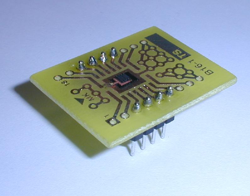
I have been investigating into copy protection mechanisms in different microcontrollers since 1996. PIC16F84 was one of the first microcontrollers I have unprotected. Occasionally I do some research in this area and provide testing of new microcontrollers and renew testing of old.
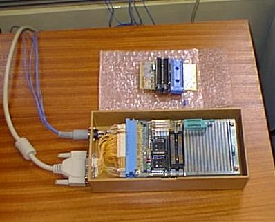
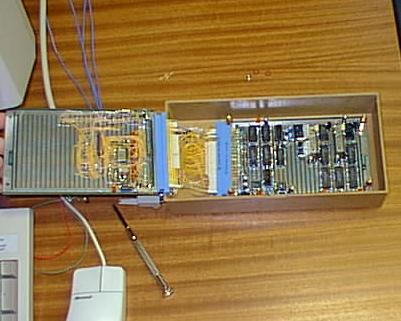
Now let me introduce what sort of equipment I have been using for non-invasive attacks on microcontrollers. I built my own designed programmer device controlled by my software program. It operates on IBM PC under MS-DOS or Windows 95/98 and it was written in C++. Hardware of my programmer allows me to rapidly change power supply and programming voltages in wide range causing different power glitches. This is quite essential if you provide attacks on microcontrollers. Signal block of the programmer generates 32 output digital signals with adjustable logic levels and some of them has open-drain output. Also this block inputs 16 signals at correct logic levels. This is quite enough for most of microcontrollers. Another part of the programmer is the board with different IC sockets for most of microcontrollers I have tested. For some microcontrollers I use additional socket adapters.
Here is some pictures of my device.
The next table shows all microcontrollers I have already tested and found them vulnerable for non-invasive attacks.
| Microcontroller |
Features |
Attack method |
Comments |
Motorola HC05
MC68HC05B6
MC68HC05B8
MC68HC05B16
(MC68HC05B32)
(MC68HC05X4)
MC68HC05X16
MC68HC05X32 |
Mask ROM
Data EEPROM
EEPROMed Security bit shared with Data memory |
Power Glitch or
Clock Glitch |
Have Write Protection against accidental Erase of Data memory |
Motorola HC11
MC68HC11A8
MC68HC11E9
(MC68HC11E20)
MC68HC11L6
(MC68HC11KA2)
(MC68HC11KA4)
(MC68HC11KG2)
(MC68HC11KG4) |
Mask ROM
Data EEPROM
EEPROMed Security bit |
Power Glitch |
Bootloader with autoerasing of the Data memory if Security is enabled |
Microchip PIC
PIC16C84 |
Program EEPROM
Data EEPROM
EEPROMed Security bit |
Power Overstress or
Power Glitch |
Chip Erase mode erases CP bits with Program and Data memories |
Microchip PIC
PIC16F83
PIC16F84
HCS512 |
Program Flash EPROM
Data EEPROM
EEPROMed Security Bit |
Power Glitch |
Chip Erase mode erases CP bits with Program and Data memories |
Microchip PIC
PIC16F84A
PIC16F627
PIC16F628
(PIC16F870)
(PIC16F871)
(PIC16F872)
PIC16F873
PIC16F874
PIC16F876
PIC16F877 |
Program Flash EPROM
Data EEPROM
EEPROMed Security Bits |
Power Glitch |
Chip Erase mode erases CP bits with Program and Data memories
Have improved protection mechanism |
Atmel 8051
AT89C51
AT89C52
AT89C55
AT89C1051
AT89C2051
(AT89C4051) |
Program Flash EPROM
EEPROMed Security Bits |
Power Glitch |
Chip Erase mode erases Lock bits with Program memory |
Atmel AVR
AT90S1200
AT90S2313
AT90S2323
(AT90S2343)
AT90S8515 |
Program Flash EPROM
Data EEPROM
EEPROMed Security Bits |
Power Glitch |
Chip Erase mode erases Lock bits with Program and Data memories |
NEC 78K/0S
(uPD78F9026)
(uPD78F9046)
uPD78F9116
(uPD78F9136) |
Program Flash EPROM
No Memory Read Function |
Power Glitch |
Chip Erase mode erases Program memory |
Texas Instruments MSP430
MSP430F110
MSP430F112
MSP430F1101
MSP430F1121
MSP430F122
MSP430F123
MSP430F133
MSP430F135
MSP430F147
MSP430F148
MSP430F149
MSP430F412
MSP430F413 |
Program Flash EPROM
Data Flash EPROM
EEPROMed Password |
Clock Glitch |
Mass Erase mode erases Password with Program and Data memories |
| Microcontroller in brackets means it has not been tested yet but expecting the same behaviour |
| Presense of a microcontroller in this table only means that it has some vulnerabilities to non-invasive attacks. It might be possible that newer versions of the same microcontroller do not have such security problems |
For some microcontrollers I know a few methods to overcome protection. Some of them give very reliable results, another has less than 20% of success (these methods sometimes appear in the Internet and, moreover, using these methods you could not only burn the chip but programmer unit too).
Invasive Attacks on Microcontrollers
WARNING! I don't care any responsibility of using further information in order to break your microcontroller. It is only brief short explanation of my experiments. If you are trying to repeat this work you are doing it on your own risk!
1. Introduction
It is commonly believed that invasive attacks are very complicated and require a lot of sophisticated equipment. It is not the case. Of course invasive attacks should cost more than non-invasive because involve depackaging of the chip and applying different physical methods. But sometimes they could be done quite easily without using expensive laboratory equipment. It reveals a huge threat to a device based on microcontroller which was assumed to be strong to non-invasive attacks but nothing related with invasive attacks was evaluated.
Let me break the myth which says that the minimum cost of invasive attack is ten thousand US$, therefore if microcontroller you use is not vulnerable to non-invasive attack you have proper protection against copying of your code. The aim is to make developers to be aware that proper evaluation should be performed before using certain microcontroller.
Let me show how PIC12C508A device could be broken and then you can estimate how difficult it is and how much could it cost. Then I will introduce an attack on PIC16F874 which requires more equipment but could be done using only microscope with probing needle.
2. Attack on PIC12C508A
Firstly we have to depackage the chip. It could be done in two ways: dissolving everything around the chip or removing plastic only above the silicon die. The last one is more intelligent but requires some level of knowledge and experience, while the first way will force you to bond the chip on a test package and it is not possible to carry out it without having access to a bonding station.
So the only convenient way for us is to remove plastic above the chip die. It is possible to do this using fuming nitric acid which dissolves epoxy plastic (material of the package) without affecting the chip and bonding wires. Exhausted acid should be removed by an acetone followed by cleaning the sample in an ultrasonic bath, wash in water to remove remain salts and drying. If you do not have an ultrasonic bath you can skip this operation. In this case the chip surface will remain slightly dirty but it still be transparent to UV light. Meanwhile the ultrasonic bath could be easily built using simple frequency generator connected to ferrite antenna coil and appropriate metal dish for bath.
Here is some pictures of this process.
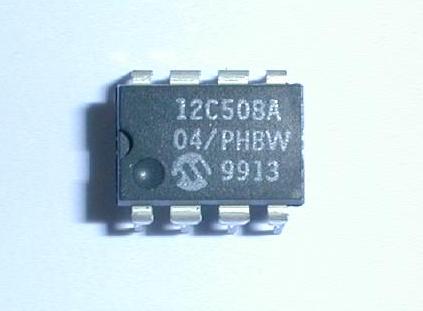 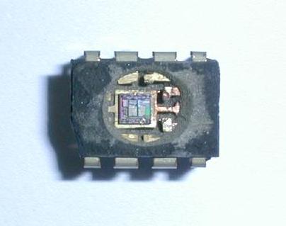   
Next stage is to expose protection fuses to UV light. In order to do this you have to find where they are. If you have a microscope with at least 100x magnification you can easily find them just tracing the wire from the pin for programming voltage input. If you do not have a microscope you can do simple search exposing different part of the chip to UV light and observing the result. Once you have found them you can apply it to protected chip. You should use opaque paper in order to protect Program memory from UV light. Five to ten minutes under UV light should give you proper result and you would be able to read Program memory using any available programmer unit.
Another possible attack requires additional equipment like microscope and laser cutter/thin needle. Once you have found protection fuse you can find all signal lines coming to this part of circuit. Due to design mistake it is possible to disable copy protection just by cutting one line from protection fuse to rest of the circuit. For unknown reason this line is sufficiently far away from other lines. That makes possible to cut this line not only using expensive laser cutter but also scratching surface above this line by a needle until the wire will be cut.
3. Attack on PIC16F874
First stage - depackaging is absolutely the same as for PIC12C508A.
Because this chip uses shielded EEPROM cells for protection it is not possible to reset protection using a UV light. So we should try to use microprobing technique in order to read the memory contents. Once you have depackaged the chip you should look onto it under a microscope. You can easily find data lines going from memory array to rest of the circuit. For unknown reason copy protection doesn't lock access to the memory in programming mode so if you put probing needle on top of the data line you will see all necessary data. Restarting read operation in programming mode and connecting probing needle to different data lines you can read all the information from both Program and Data memories.
Threat of Attack and Defense Technologies
Now having information about different attack methods we can divide these attacks by threat to device based on microcontroller.
Non-invasive attacks introduce very high level of threat therefore if microcontroller is vulnerable to such attacks it has minimum level of protection. The only equipment which attacker should have is a special programmer unit. For example, you can find such programmer units for PIC16C84 widely available for sale in the Internet for quite reasonable price.
Cheap invasive attacks also reveal big problem to designers. These attacks could be implemented by practically any person familiar with school chemistry course. All necessary equipment could be bought for 100 to 300 US$. And microcontrollers vulnerable to such attacks could not be enough secure.
Such invasive attacks as microprobing could be used only by well funded attackers. It makes microcontrollers vulnerable only to these attacks to be enough secured. But also, if you calculate price of equipment and time to break one microcontroller you will get price of attack not exceeding one thousand US$. So you cannot use such microcontrollers in expensive project where protection is the necessary requirement.
Reverse engineering is the most expensive invasive attack could be used. It gives all the necessary information about chip schematics and structure of protection circuit. But it takes long time and require very expensive equipment. So if microcontroller could not be broken by any of above mentioned attacks it should be good secured. Although maybe it was not broken due to mistake of attacker and other attacker could break it quite easily.
Now we get very awful situation where practically any standard microcontroller could be broken using one of the first three attack methods. Usually it is not possible to redesign project for secure microcontroller which can withstand practically any attack because of high price of such microcontrollers and incompatibility with ordinary microcontrollers. Usually secure microcontrollers are designed for smartcard applications where used only two pins for serial digital interface. Of course, you can use secure microcontroller to protect the project but if attacker interested only in certain part of the algorithm implemented in normal microcontroller he can extract it without a problem.
Another approach is to use hardware protection based on a programmable logic array (PAL, CPLD, EPLD) which usually has better protection and even if you break it you will spend a lot of time to understand how it works.
But why not to use undocumented features of the same microcontroller. If you are using OTP, UV EPROM, EEPROM or Flash microcontroller it is possible to use certain cells of its memory for protection. The idea behind this is the next. All these memories are analog memory, so each cell inside the array keeps charge instead of logic state. When memory cell is read this charge is translated into a logic signal by sense amplifier. If you charge cell to intermediate state corresponds to threshold value of sense amplifier then because of presence of a noise you will read different value from the same cell. This feature could be used as additional protection to ordinary security feature of a microcontroller.
Another possible way of increasing protection is to destroy possibility of further programming. It could be done mechanically by cutting certain pins or electrically by applying high voltage to these pins to blow up bonding wire. Although it does not provide any protection against invasive attacks.
More intelligent way is to destroy certain part of the control circuit dedicated for programming mode. Although in order to do such a thing you should reverse engineer certain part of the chip or apply microprobing technique to learn how it works. But sometimes it might cost more than the value of your project.
Further Research
The other interesting way of research is evaluation of the security in Programmable Logic Arrays (PLA) and Programmable Logic Devices (PLD). They also have security protection feature but it was not tested by the same methods like microcontrollers. Sometimes this devices are used for complex projects in parallel to FPGA chips but only to prevent unauthorised copying because FPGA chip does not have any protection facility due to external loading of configuration. In this case attacks on EEPROMed PLA/PLD also could be serious threat for such devices.
|