If MikaTech was a bad company, you could find tons of bad reputations about its service on the internet over the 28 years history
So, the answer is YES! We are good people.Why choose Mikatech, please click here to find out
 MikaTech Lab - Slide
 MikaTech Lab Started
 MCU Decap Room
About MikaTech
Time went fast, from the day we did our first 8051 MCU reverse engineering project in 1998, to the day we set up our million dollar reverse engineering lab in 2012, 14 years went by. Now we start our new business of embedded visual system development, hope we can serve another 10 years.
 Peter Lee
Co-Founder & CEO
Peter Lee
Co-Founder & CEO
 Operating purely as an intellectual property (IP) vendor, ARM Holdings never fabricates physical semiconductor chips on its own. Instead, the company commercializes its processor blueprints by issuing design licences to external semiconductor manufacturers across the industry. A wide range of modern system-on-chip (SoC) products adopt ARM processor cores, including Qualcomm Snapdragon, NVIDIA Tegra, Marvell XScale, and Texas Instruments OMAP platforms, alongside ARM’s own Cortex processor family and Apple custom SoC silicon deployed inside iPhone devices. The term ARM began as an abbreviation for Acorn RISC Machine[6]; following the phasing out of the Acorn brand name, the definition was rebranded to stand for Advanced RISC Machine.
Built upon fundamental RISC design principles, ARM processor hardware requires far fewer transistors than conventional complex instruction set computing (CISC) processors used in traditional desktop computers. This simplified hardware structure delivers major advantages including lower manufacturing cost, decreased thermal output, and drastically reduced power consumption. These characteristics make ARM architectures uniquely suitable for lightweight, portable, battery-reliant devices such as smartphones and tablet computers.[7] Thanks to its streamlined complexity, designers can integrate ARM cores into compact, low-power embedded systems-on-chip that combine onboard memory, peripheral interfaces, wireless radio modules, and other functional components. The Apple Newton personal digital assistant (PDA) served as one of the earliest commercial examples of this design methodology, while the same optimization philosophy underpins the Apple A4 and A5 processors utilized in early iPad generations. Beyond mobile embedded devices, the inherent simplicity of RISC-based ARM designs also enables cost-effective multi-core CPU implementations. Engineers can deploy higher core densities with improved energy efficiency, delivering stronger overall computational performance for modern servers, laptops, and portable notebook computing platforms.
Operating purely as an intellectual property (IP) vendor, ARM Holdings never fabricates physical semiconductor chips on its own. Instead, the company commercializes its processor blueprints by issuing design licences to external semiconductor manufacturers across the industry. A wide range of modern system-on-chip (SoC) products adopt ARM processor cores, including Qualcomm Snapdragon, NVIDIA Tegra, Marvell XScale, and Texas Instruments OMAP platforms, alongside ARM’s own Cortex processor family and Apple custom SoC silicon deployed inside iPhone devices. The term ARM began as an abbreviation for Acorn RISC Machine[6]; following the phasing out of the Acorn brand name, the definition was rebranded to stand for Advanced RISC Machine.
Built upon fundamental RISC design principles, ARM processor hardware requires far fewer transistors than conventional complex instruction set computing (CISC) processors used in traditional desktop computers. This simplified hardware structure delivers major advantages including lower manufacturing cost, decreased thermal output, and drastically reduced power consumption. These characteristics make ARM architectures uniquely suitable for lightweight, portable, battery-reliant devices such as smartphones and tablet computers.[7] Thanks to its streamlined complexity, designers can integrate ARM cores into compact, low-power embedded systems-on-chip that combine onboard memory, peripheral interfaces, wireless radio modules, and other functional components. The Apple Newton personal digital assistant (PDA) served as one of the earliest commercial examples of this design methodology, while the same optimization philosophy underpins the Apple A4 and A5 processors utilized in early iPad generations. Beyond mobile embedded devices, the inherent simplicity of RISC-based ARM designs also enables cost-effective multi-core CPU implementations. Engineers can deploy higher core densities with improved energy efficiency, delivering stronger overall computational performance for modern servers, laptops, and portable notebook computing platforms.
 STM32F100V STM32F101 STM32F103 STM32F105 STM32F107RC STM32L151 STM32L152 STM32F205 STM32F207 STM32F215 STM32F217 STM32F405 STM32F407 STM32F415 STM32F417 STM32L151 STM32L152 STM32F101RE STM32F101RD STM32F205RC STM32F101VE STM32F101VD STM32F100RE STM32F103RE STM32F100VE STM32F100RD STM32F103RD STM32F100VD STM32F103VD STM32F100ZD STM32F205VC STM32F207VC STM32F205ZC STM32F105VC STM32F105RC STM32F101RC STM32F107RC STM32F101VC STM32F107VC STM32F101ZC STM32F100RC STM32F103RC STM32F100VC STM32F103VC STM32F100ZC STM32F205RB STM32L151CB STM32L152CB STM32L151RB STM32L152RB STM32F205VB STM32L15VB STM32F105VB STM32L152VB STM32F103ZC STM32F103TB STM32F101CB STM32F103CB STM32F101RB STM32F103RB STM32F101VB STM32F107VB STM32F101TB STM32F100CC STM32F102CB STM32F100RB STM32F102RB STM32F100VB STM32F103VB STM32L151C8 STM32L152C8 STM32F103C8 STM32F102C8 STM32L152C6 STM32F103C6 STM32F102C6 STM32F103C4 STM32F102C4 STM32L151R8 STM32F105R8 STM32F103T8 STM32F101T8 STM32F101C8 STM32F100C8 STM32L151C6 STM32F101R8 STM32F100R8 STM32L151R6 STM32F101R6 STM32F100R6 STM32F101R4 STM32F100R4 STM32F407VG STM32F417VG STM32F407ZG STM32F417ZG STM32F405RG STM32F415RG STM32F405VG STM32F415VG STM32F405ZG STM32F415ZG STM32F207VG STM32F217VG STM32F207ZG STM32F217ZG STM32F205RG STM32F215RG STM32F205VG STM32F215VG STM32F205ZG STM32F215ZG STM32F101RG STM32F103RG STM32F101VG STM32F103VG STM32F101ZG STM32F103ZG STM32F205RF STM32F101RF STM32F103RF STM32F205VF STM32F101VF STM32F407VE STM32F207VE STM32F207VF STM32F103VF STM32F417VE STM32F217VE STM32F215VE STM32F103VE STM32F205ZF STM32F101ZF STM32F407ZE STM32F207ZE STM32F205ZE STM32F101ZE STM32F100ZE STM32F101ZD STM32F103ZD STM32F207ZC STM32F207IC STM32F103VE STM32F207ZF STM32F103ZF STM32F417ZE STM32F217ZE STM32F215ZE STM32F407IE STM32F207IE STM32F417IE STM32F217IE STM32F207IF STM32F207IG STM32F217IG STM32F407IG STM32F417IG STM32F205RE STM32F215RE STM32F205VE ...
ARM microprocessor cores[edit source | edit]Designed by ARM[edit source | edit]ARM Family ARM Architecture ARM Core Feature Cache (I/D), MMU Typical MIPS @ MHz
ARM1 ARMv1 ARM1 First implementation None
ARM2 ARMv2 ARM2 ARMv2 added the MUL (multiply) instruction None 4 MIPS @ 8 MHz
0.33 DMIPS/MHz
ARMv2a ARM250 Integrated MEMC (MMU), Graphics and IO processor. ARMv2a added the SWP and SWPB (swap) instructions. None, MEMC1a 7 MIPS @ 12 MHz
ARM3 ARMv2a ARM3 First integrated memory cache. 4 KB unified 12 MIPS @ 25 MHz
0.50 DMIPS/MHz
ARM6 ARMv3 ARM60 ARMv3 first to support 32-bit memory address space (previously 26-bit) None 10 MIPS @ 12 MHz
ARM600 As ARM60, cache and coprocessor bus (for FPA10 floating-point unit). 4 KB unified 28 MIPS @ 33 MHz
ARM610 As ARM60, cache, no coprocessor bus. 4 KB unified 17 MIPS @ 20 MHz
0.65 DMIPS/MHz
ARM7 ARMv3 ARM700 8 KB unified 40 MHz
ARM710 As ARM700, no coprocessor bus. 8 KB unified 40 MHz
ARM710a As ARM710 8 KB unified 40 MHz
0.68 DMIPS/MHz
ARM7TDMI ARMv4T ARM7TDMI(-S) 3-stage pipeline, Thumb none 15 MIPS @ 16.8 MHz
63 DMIPS @ 70 MHz
ARM710T As ARM7TDMI, cache 8 KB unified, MMU 36 MIPS @ 40 MHz
ARM720T As ARM7TDMI, cache 8 KB unified, MMU with Fast Context Switch Extension 60 MIPS @ 59.8 MHz
ARM740T As ARM7TDMI, cache MPU
ARM7EJ ARMv5TEJ ARM7EJ-S 5-stage pipeline, Thumb, Jazelle DBX, Enhanced DSP instructions none
ARM8 ARMv4 ARM810[4][5] 5-stage pipeline, static branch prediction, double-bandwidth memory 8 KB unified, MMU 84 MIPS @ 72 MHz
1.16 DMIPS/MHz
ARM9TDMI ARMv4T ARM9TDMI 5-stage pipeline, Thumb none
ARM920T As ARM9TDMI, cache 16 KB/16 KB, MMU with FCSE (Fast Context Switch Extension)[6] 200 MIPS @ 180 MHz
ARM922T As ARM9TDMI, caches 8 KB/8 KB, MMU
ARM940T As ARM9TDMI, caches 4 KB/4 KB, MPU
ARM9E ARMv5TE ARM946E-S Thumb, Enhanced DSP instructions, caches variable, tightly coupled memories, MPU
ARM966E-S Thumb, Enhanced DSP instructions no cache, TCMs
ARM968E-S As ARM966E-S no cache, TCMs
ARMv5TEJ ARM926EJ-S Thumb, Jazelle DBX, Enhanced DSP instructions variable, TCMs, MMU 220 MIPS @ 200 MHz
ARMv5TE ARM996HS Clockless processor, as ARM966E-S no caches, TCMs, MPU
ARM10E ARMv5TE ARM1020E 6-stage pipeline, Thumb, Enhanced DSP instructions, (VFP) 32 KB/32 KB, MMU
ARM1022E As ARM1020E 16 KB/16 KB, MMU
ARMv5TEJ ARM1026EJ-S Thumb, Jazelle DBX, Enhanced DSP instructions, (VFP) variable, MMU or MPU
ARM11 ARMv6 ARM1136J(F)-S[7] 8-stage pipeline, SIMD, Thumb, Jazelle DBX, (VFP), Enhanced DSP instructions variable, MMU 740 @ 532–665 MHz (i.MX31 SoC), 400–528 MHz
ARMv6T2 ARM1156T2(F)-S 8-stage pipeline, SIMD, Thumb-2, (VFP), Enhanced DSP instructions variable, MPU
ARMv6Z ARM1176JZ(F)-S As ARM1136EJ(F)-S variable, MMU + TrustZone 965 DMIPS @ 772 MHz, up to 2 600 DMIPS with four processors[8]
ARMv6K ARM11 MPCore As ARM1136EJ(F)-S, 1–4 core SMP variable, MMU
SecureCore ARMv6-M SC000 0.9 DMIPS/MHz
ARMv4T SC100
ARMv7-M SC300 1.25 DMIPS/MHz
Cortex-M ARMv6-M Cortex-M0 [9] Microcontroller profile, Thumb + Thumb-2 subset (BL, MRS, MSR, ISB, DSB, DMB),[10] hardware multiply instruction (optional small), optional system timer, optional bit-banding memory No cache, No TCM, No MPU 0.84 DMIPS/MHz
Cortex-M0+ [11] Microcontroller profile, Thumb + Thumb-2 subset (BL, MRS, MSR, ISB, DSB, DMB),[10] hardware multiply instruction (optional small), optional system timer, optional bit-banding memory No cache, No TCM, optional MPU with 8 regions 0.93 DMIPS/MHz
Cortex-M1 [12] Microcontroller profile, Thumb + Thumb-2 subset (BL, MRS, MSR, ISB, DSB, DMB),[10] hardware multiply instruction (optional small), OS option adds SVC / banked stack pointer, optional system timer, no bit-banding memory No cache, 0-1024 KB I-TCM, 0-1024 KB D-TCM, No MPU 136 DMIPS @ 170 MHz,[13] (0.8 DMIPS/MHz FPGA-dependent)[14]
ARMv7-M Cortex-M3 [15] Microcontroller profile, Thumb / Thumb-2, hardware multiply and divide instructions, optional bit-banding memory No cache, No TCM, optional MPU with 8 regions 1.25 DMIPS/MHz
ARMv7E-M Cortex-M4 [16] Microcontroller profile, Thumb / Thumb-2 / DSP / optional FPv4 single-precision FPU, hardware multiply and divide instructions, optional bit-banding memory No cache, No TCM, optional MPU with 8 regions 1.25 DMIPS/MHz
Cortex-R ARMv7-R Cortex-R4 [17] Real-time profile, Thumb / Thumb-2 / DSP / optional VFPv3 FPU, hardware multiply and optional divide instructions, optional parity & ECC for internal buses / cache / TCM, 8-stage pipeline dual-core running lockstep with fault logic 0-64 KB / 0-64 KB, 0-2 of 0-8 MB TCM, opt MPU with 8/12 regions
Cortex-R5 (MPCore) [18] Real-time profile, Thumb / Thumb-2 / DSP / optional VFPv3 FPU and precision, hardware multiply and optional divide instructions, optional parity & ECC for internal buses / cache / TCM, 8-stage pipeline dual-core running lock-step with fault logic / optional as 2 independent cores, low-latency peripheral port (LLPP), accelerator coherency port (ACP) [19] 0-64 KB / 0-64 KB, 0-2 of 0-8 MB TCM, opt MPU with 12/16 regions
Cortex-R7 (MPCore) [20] Real-time profile, Thumb / Thumb-2 / DSP / optional VFPv3 FPU and precision, hardware multiply and optional divide instructions, optional parity & ECC for internal buses / cache / TCM, 11-stage pipeline dual-core running lock-step with fault logic / out-of-order execution / dynamic register renaming / optional as 2 independent cores, low-latency peripheral port (LLPP), ACP [19] 0-64 KB / 0-64 KB, ? of 0-128 KB TCM, opt MPU with 16 regions
Cortex-A ARMv7-A Cortex-A5 [21] Application profile, ARM / Thumb / Thumb-2 / DSP / SIMD / Optional VFPv4-D16 FPU / Optional NEON / Jazelle RCT and DBX, 1–4 cores / optional MPCore, snoop control unit (SCU), generic interrupt controller (GIC), accelerator coherence port (ACP) 4-64 KB / 4-64 KB L1, MMU + TrustZone 1.57 DMIPS / MHz per core
Cortex-A7 MPCore [22] Application profile, ARM / Thumb / Thumb-2 / DSP / VFPv4-D16 FPU / NEON / Jazelle RCT and DBX / Hardware virtualization, in-order execution, superscalar, 1–4 SMP cores, Large Physical Address Extensions (LPAE), snoop control unit (SCU), generic interrupt controller (GIC), ACP, architecture and feature set are identical to A15, 8-10 stage pipeline, low-power design[23] 32 KB / 32 KB L1, 0-4 MB L2, L1 & L2 have Parity & ECC, MMU + TrustZone 1.9 DMIPS / MHz per core
Cortex-A8 [24] Application profile, ARM / Thumb / Thumb-2 / VFPv3 FPU / NEON / Jazelle RCT and DAC, 13-stage superscalar pipeline 16-32 KB / 16-32 KB L1, 0-1 MB L2 opt ECC, MMU + TrustZone up to 2000 (2.0 DMIPS/MHz in speed from 600 MHz to greater than 1 GHz)
Cortex-A9 MPCore [25] Application profile, ARM / Thumb / Thumb-2 / DSP / Optional VFPv3 FPU / Optional NEON / Jazelle RCT and DBX, out-of-order speculative issue superscalar, 1–4 SMP cores, snoop control unit (SCU), generic interrupt controller (GIC), accelerator coherence port (ACP) 16-64 KB / 16-64 KB L1, 0-8 MB L2 opt Parity, MMU + TrustZone 2.5 DMIPS/MHz per core, 10,000 DMIPS @ 2 GHz on Performance Optimized TSMC 40G (dual core)
ARM Cortex-A12 [26] Application profile, ARM / Thumb-2 / DSP / VFPv4 FPU / NEON / Hardware virtualization, out-of-order speculative issue superscalar, 1–4 SMP cores, Large Physical Address Extensions (LPAE), snoop control unit (SCU), generic interrupt controller (GIC), accelerator coherence port (ACP) 32-64KB / 32 KB L1, 256KB-8 MB L2 3.0 DMIPS / MHz per core
Cortex-A15 MPCore [27] Application profile, ARM / Thumb / Thumb-2 / DSP / VFPv4 FPU / NEON / Jazelle RCT / Hardware virtualization, out-of-order speculative issue superscalar, 1–4 SMP cores, Large Physical Address Extensions (LPAE), snoop control unit (SCU), generic interrupt controller (GIC), ACP, 15-24 stage pipeline[23] 32 KB / 32 KB L1, 0-4 MB L2, L1 & L2 have Parity & ECC, MMU + TrustZone At least 3.5 DMIPS/MHz per core (Up to 4.01 DMIPS/MHz depending on implementation).[28]
Cortex-A50 ARMv8-A Cortex-A53[29] Application profile, AArch32 and AArch64, 1-4 SMP cores, Trustzone, NEON advanced SIMD, VFPv4, hardware virtualization, dual issue, in-order pipeline 8~64 KB/8~64 KB L1 per core, 128 KB~2 MB L2 shared, 40-bit physical addresses 2.3 DMIPS/MHz
Cortex-A57[30] Application profile, AArch32 and AArch64, 1-4 SMP cores, Trustzone, NEON advanced SIMD, VFPv4, hardware virtualization, multi-issue, deeply out-of-order pipeline 48 KB/32 KB L1 per core, 512 KB~2 MB L2 shared, 44-bit physical addresses At least 4.1 DMIPS/MHz per core (Up to 4.76 DMIPS/MHz depending on implementation).
ARM Family ARM Architecture ARM Core Feature Cache (I/D), MMU Typical MIPS @ MHz
Designed by third parties[edit source | edit]These cores implement the ARM instruction set, and were developed independently by companies with an architectural license from ARM.
Family ARM Architecture Core Feature Cache (I/D), MMU Typical MIPS @ MHz
StrongARM ARMv4 SA-1 5-stage pipeline 16 KB/8–16 KB, MMU 133–206 MHz
1.0 DMIPS/MHz
Faraday[31] ARMv4 FA510 6-stage pipeline up to 32 KB / 32 KB Cache, MPU 1.26 DMIPS/MHz
100-200 MHz
FA526 up to 32 KB / 32 KB Cache, MMU 1.26 MIPS/MHz
166-300 MHz
FA626 8-stage pipeline 32 KB/32 KB Cache, MMU 1.35 DMIPS/MHz
500 MHz
ARMv5TE FA606TE 5-stage pipeline no cache, no MMU 1.22 DMIPS/MHz
200 MHz
FA626TE 8-stage pipeline 32 KB/32 KB Cache, MMU 1.43 MIPS/MHz
800 MHz
FMP626TE 8-stage pipeline, SMP 1.43 MIPS/MHz
500 MHz
FA726TE 13 stage pipeline, dual issue 2.4 DMIPS/MHz
1000 MHz
XScale ARMv5TE XScale 7-stage pipeline, Thumb, Enhanced DSP instructions 32 KB/32 KB, MMU 133–400 MHz
Bulverde Wireless MMX, Wireless SpeedStep added 32 KB/32 KB, MMU 312–624 MHz
Monahans[32] Wireless MMX2 added 32 KB/32 KB (L1), optional L2 cache up to 512 KB, MMU up to 1.25 GHz
Sheeva ARMv5 Feroceon 5-8 stage pipeline, single-issue 16 KB / 16 KB, MMU 600-2000 MHz
Jolteon 5-8 stage pipeline, dual-issue 32 KB / 32 KB, MMU
PJ1 (Mohawk) 5-8 stage pipeline, single-issue, Wireless MMX2 32 KB / 32 KB, MMU 1.46 DMIPS/MHz
1.06 GHz
ARMv6/ARMv7-A PJ4 6-9 stage pipeline, dual-issue, Wireless MMX2, SMP 32 KB / 32 KB, MMU 2.41 DMIPS/MHz
1.6 GHz
Snapdragon ARMv7-A Scorpion [33] 1 or 2 cores. ARM / Thumb / Thumb-2 / DSP / SIMD / VFPv3 FPU / NEON (128-bit wide) 256 KB L2 per core 2.1 DMIPS / MHz per core
Krait [33] 1, 2, or 4 cores. ARM / Thumb / Thumb-2 / DSP / SIMD / VFPv4 FPU / NEON (128-bit wide) 4 KB / 4 KB L0, 16 KB / 16 KB L1, 512 KB L2 per core 3.3 DMIPS / MHz per core
Apple Ax ARMv7-A Apple Swift [34] 2 cores. ARM / Thumb / Thumb-2 / DSP / SIMD / VFPv4 FPU / NEON L1: 32 kB instruction + 32 kB data, L2: 1 MB 3.5 DMIPS / MHz Per Core
X-Gene ARMv8-A X-Gene 64 bit, quad issue, SMP Cache, MMU, Virtualization 3 GHz
Denver ARMv8-A Parker 64 bit
See also[edit source | edit] Computer science portal
Electronics portal
ARM architecture
List of applications of ARM cores
References[edit source | edit]^ "Line Card" (PDF). 2003. Retrieved 2011-01-06.
^ ARM Ltd and ARM Germany GmbH. "Device Database". Keil. Retrieved 2011-01-06.
^ "Processors". ARM. 2011. Retrieved 2011-01-06.
^ ARM Holdings (1996-08-07), ARM810 – Dancing to the Beat of a Different Drum (PDF), Hot Chips .
^ "VLSI Technology Now Shipping ARM810". EE Times. August 26, 1996. Retrieved March 16, 2012.
^ Register 13, FCSE PID register ARM920T Technical Reference Manual
^ "ARM1136J(F)-S – ARM Processor". Arm.com. Retrieved 2009-04-18.
^ "ARM11 Processor Family". ARM. Retrieved 2010-12-13.
^ Cortex-M0 Specification Summary; ARM Holdings.
^ a b c Cortex-M0/M0+/M1 Instruction Set; ARM Holding.
^ Cortex-M0+ Specification Summary; ARM Holdings.
^ Cortex-M1 Specification Summary; ARM Holdings.
^ "ARM Extends Cortex Family with First Processor Optimized for FPGA", ARM press release, March 19, 2007. Retrieved April 11, 2007.
^ "ARM Cortex-M1", ARM product website. Retrieved April 11, 2007.
^ Cortex-M3 Specification Summary; ARM Holdings.
^ Cortex-M4 Specification Summary; ARM Holdings.
^ Cortex-R4 Specification Summary; ARM Holdings.
^ Cortex-R5 Specification Summary; ARM Holdings.
^ a b Cortex-R5 & Cortex-R7 Press Release; ARM Holdings; January 31, 2011.
^ Cortex-R7 Specification Summary; ARM Holdings.
^ Cortex-A5 Specification Summary; ARM Holdings.
^ Cortex-A7 Specification Summary; ARM Holdings.
^ a b Deep inside ARM's new Intel killer; The Register; October 20, 2011.
^ Cortex-A8 Specification Summary; ARM Holdings.
^ Cortex-A9 Specification Summary; ARM Holdings.
^ Cortex-A12 Summary; ARM Holdings.
^ Cortex-A15 Specification Summary; ARM Holdings.
^ Exclusive : ARM Cortex-A15 "40 Per Cent" Faster Than Cortex-A9 | ITProPortal.com
^ "Cortex-A53 Processor". ARM Holdings. Retrieved 2012-10-13.
^ "Cortex-A57 Processor". ARM Holdings. Retrieved 2012-10-13.
^ [1]
^ "3rd Generation Intel XScale Microarchitecture: Developer’s Manual". download.intel.com. Intel. May 2007. Retrieved 2 December 2010.
^ a b Qualcomm's New Snapdragon S4: MSM8960 & Krait Architecture Explored; Anandtech.
^ Lal Shimpi, Anand (September 15, 2012). "The iPhone 5's A6 SoC: Not A15 or A9, a Custom Apple Core Instead". AnandTech. Retrieved September 15, 2012.
Further reading[edit source | edit]The Definitive Guide to the ARM Cortex-M0; 1st Edition; Joseph Yiu; Newnes; 552 pages; 2011; ISBN 978-0-12-385477-3. (Online Sample)
The Definitive Guide to the ARM Cortex-M3; 2nd Edition; Joseph Yiu; Newnes; 480 pages; 2009; ISBN 978-1-85617-963-8. (Online Sample)
[hide]v t eARM-based chips
ARM architecture List of ARM microprocessor cores
Application
Processors Cortex-A5 Actions ATM7025/7029 Qualcomm Snapdragon S4 Play/200 InfoTMIC iMAPx820/iMAPx15 Telechips TCC892x
Cortex-A7 Allwinner A20/A31s/A31 HiSilicon K3V3 Leadcore LC1813 MediaTek MT6572/6589/6589T/6589M/8125/6599 Qualcomm Snapdragon 200/400 Samsung Exynos 5410
Cortex-A8 Allwinner A10/A13/A10s Apple A4 Freescale i.MX5x Rockchip RK290x/RK291x Samsung Exynos 3110/S5PC110/S5PV210 Texas Instruments OMAP 3 ZiiLABS ZMS-08
Cortex-A9 Amlogic AML8726 Apple A5/A5X Freescale i.MX6x HiSilicon K3V2/K3V2T/K3V2E MediaTek MT6575/6577 Nvidia Tegra 2/3/4i Nufront NuSmart 2816M/NS115/NS115M Renesas EMMA EV2 Rockchip RK292x/RK30xx/RK31xx Samsung Exynos 4 ST-Ericsson NovaThor Telechips TCC8803 Texas Instruments OMAP 4 VIA WonderMedia WM88x0/89x0 ZiiLABS ZMS-20, ZMS-40
Cortex-A15 HiSilicon K3V3 MediaTek MT6599 Nvidia Tegra 4 Samsung Exynos 5 Texas Instruments OMAP 5
ARMv7-A
compatible Apple A6/A6X (Swift) Qualcomm Snapdragon S1/S2/S3 (Scorpion) Qualcomm Snapdragon S4 Plus/S4 Pro (Krait) Qualcomm Snapdragon 600/800 (Krait 300/Krait 400) Marvell P4J
Embedded
Microcontrollers Cortex-M0 Energy Micro EFM32 Zero NXP LPC1100, LPC1200 STMicroelectronics STM32 F0
Cortex-M0+ Freescale Kinetis L NXP LPC800
Cortex-M1 Actel FPGAs Altera FPGAs Xilinx FPGAs
Cortex-M3 Actel SmartFusion, SmartFusion 2 Atmel AT91SAM3 Cypress PSoC 5 Energy Micro EFM32 Tiny, Gecko, Leopard, Giant Fujitsu FM3 NXP LPC1300, LPC1700, LPC1800 Silicon Labs Precision32 STMicroelectronics STM32 F1, F2, L1, W Texas Instruments F28, LM3, TMS470, OMAP 4 Toshiba TX03
Cortex-M4 Atmel AT91SAM4 Freescale Kinetis K Texas Instruments OMAP 5
Cortex-M4F Energy Micro EFM32 Wonder Freescale Kinetis K Infineon XMC4000 NXP LPC4000, LPC4300 STMicroelectronics STM32 F3, F4 Texas Instruments LM4F
Real-Time
Microcontrollers Cortex-R4F Texas Instruments RM4, TMS570
Cortex-R5F Scaleo OLEA
Classic
Processors ARM7 Atmel AT91SAM7, AT91CAP7, AT91M, AT91R NXP LPC2100, LPC2200, LPC2300, LPC2400, LH7 STMicroelectronics STR7
ARMv4
compatible Digital Equipment Corporation StrongARM
ARM9 Atmel AT91SAM9, AT91CAP9 Freescale i.MX1x, i.MX2x Rockchip RK27xx/RK28xx NXP LPC2900, LPC3100, LPC3200, LH7A ST-Ericsson Nomadik STn881x STMicroelectronics STR9 Texas Instruments OMAP 1, AM1x VIA WonderMedia WM8505/8650 ZiiLABS ZMS-05
ARMv5
compatible Digital Equipment Corporation XScaleMarvell Sheeva Feroceon Jolteon Mohawk
ARM11 Broadcom BCM2835 (Raspberry Pi) Freescale i.MX3x Infotmic IMAPX210/220 Nvidia Tegra APX, 6xx Qualcomm MSM7000, Snapdragon S1 ST-Ericsson Nomadik STn882x Telechips TCC8902 TI OMAP 2 VIA WonderMedia WM87x0
ARMv6
compatible Mindspeed Comcerto 1000 .
ARM offers several microprocessor core designs, including the ARM7, ARM9, ARM11, Cortex-A8, Cortex-A9, and Cortex-A15. Companies often license these designs from ARM to manufacture and integrate into their own system on a chip (SoC) with other components including RAM, GPUs or radio basebands (for mobile phones).
System-on-chip packages integrating ARM's core designs include Nvidia Tegra's first three generations, CSR plc's Quatro family, ST-Ericsson's Nova and NovaThor, Silicon Labs's Precision32 MCU, Texas Instruments's OMAP products, Samsung's Hummingbird and Exynos products, Apple's Ax SoC line, and Freescale's i.MX.
Companies can also obtain an ARM architectural licence for designing their own CPU cores using the ARM instruction set. Distinct ARM architecture implementations by licensees include Apple's A6, AppliedMicro's X-Gene, Qualcomm's Snapdragon and Krait, DEC's StrongARM, Marvell (formerly Intel) XScale and Nvidia's planned Project Denver.
History[edit source | edit]Originally conceived by the British company Acorn Computers for use in its personal computers, the first ARM-based products were the co-processor modules for the BBC Micro series of computers. After achieving success with the BBC Micro computer, Acorn Computers considered how to move on from the relatively simple MOS Technology 6502 processor to address business markets like the one that would soon be dominated by the IBM PC, launched in 1981. The Acorn Business Computer (ABC) plan required a number of second processors to be made to work with the BBC Micro platform, but processors such as the Motorola 68000 and National Semiconductor 32016 were considered to be unsuitable, and the 6502 was not powerful enough for a graphics based user interface.[12]
After testing all of the available processors and finding them lacking, Acorn decided that it needed a new architecture. Inspired by white papers on the Berkeley RISC project, Acorn considered designing its own processor.[13] A visit to the Western Design Center in Phoenix, where the 6502 was being updated by what was effectively a single-person company, showed Acorn engineers Steve Furber and Sophie Wilson they did not need massive resources and state-of-the-art research and development facilities.[14]
Wilson developed the instruction set, writing a simulation of the processor in BBC Basic that ran on a BBC Micro with a second 6502 processor. This convinced the Acorn engineers that they were on the right track. Wilson approached Acorn's CEO, Hermann Hauser, and requested more resources. Once approval was given, a small team was assembled to implement Wilson's model in hardware.
A Conexant ARM processor used mainly in routersAcorn RISC Machine: ARM2[edit source | edit]The official Acorn RISC Machine project started in October 1983. VLSI Technology was chosen as the "silicon partner," as they were a source of ROMs and custom chips for Acorn. The design was led by Wilson and Furber, and was consciously implemented with a similar efficiency ethos as the 6502.[15] A key design goal was achieving low-latency input/output (interrupt) handling like the 6502. The 6502's memory access architecture had allowed developers to produce fast machines without using costly direct memory access hardware. VLSI produced the first ARM silicon on 26 April 1985—it worked the first time, and was known as ARM1 by April 1985.[2] The first production systems named ARM2 were available the following year.
The ARM1 second processor for the BBC MicroThe first practical application of the ARM was as a second processor for the BBC Micro, where it saw use developing the simulation software to finish development of the support chips (VIDC, IOC, MEMC), and to speed up the CAD software used in ARM2 development. Wilson subsequently rewrote BBC Basic in ARM assembly language, and the in-depth knowledge obtained from designing the instruction set enabled the code to be very dense, making ARM BBC Basic an extremely good test for any ARM emulator. The original aim of a principally ARM-based computer was achieved in 1987 with the release of the Acorn Archimedes.[16]
In 1992, Acorn once more won the Queen's Award for Technology for the ARM.
The ARM2 featured a 32-bit data bus, 26-bit address space and 27 32-bit registers. 8 bits from the program counter register were available for other purposes; the top 6 bits (available because of the 26-bit address space), served as status flags, and the bottom 2 bits (available because the program counter was always word aligned), were used for setting modes. Although the address bus was extended to 32 bits in the ARM6, program code still had to lie within the first 64 megabytes of memory in 26-bit compatibility mode, due to the reserved bits for the status flags.[17] The ARM2 had a transistor count of just 30,000, compared to Motorola's six-year-older 68000 model with 68,000.[18] Much of this simplicity came from the lack of microcode (which represents about one-quarter to one-third of the 68000) and from (like most CPUs of the day) not including any cache. This simplicity enabled low power consumption, yet better performance than the Intel 80286. A successor, ARM3, was produced with a 4 KB cache, which further improved performance.[19]
Apple, DEC, Intel, Marvell: ARM6, StrongARM, XScale[edit source | edit]In the late 1980s Apple Computer and VLSI Technology started working with Acorn on newer versions of the ARM core. In 1990, Acorn spun off the design team into a new company named Acorn RISC Machines Ltd., which became ARM Ltd when its parent company, ARM Holdings plc, floated on the London Stock Exchange and NASDAQ in 1998.[20]
The new Apple-ARM work would eventually evolve into the ARM6, first released in early 1992. Apple used the ARM6-based ARM 610 as the basis for their Apple Newton personal digital assistant (PDA). In 1994, Acorn used the ARM 610 as the main central processing unit (CPU) in their Risc PC computers. DEC licensed the ARM6 architecture and produced the StrongARM. At 233 MHz, this CPU drew only one watt (newer versions draw far less). This work was later passed to Intel as a part of a lawsuit settlement, and Intel took the opportunity to supplement their i960 line with the StrongARM. Intel later developed its own high performance implementation named XScale which it has since sold to Marvell.
Licensing[edit source | edit]The ARM core has remained essentially the same size throughout these changes. ARM2 had 30,000 transistors, the ARM6 grew only to 35,000. ARM's primary business is selling IP cores, which licensees use to create microcontrollers and CPUs based on those cores. The original design manufacturer combines the ARM core with other parts to produce a complete CPU, typically one that can be built in existing semiconductor fabs at low cost and still deliver substantial performance. The most successful implementation has been the ARM7TDMI with hundreds of millions sold. Atmel has been a precursor design center in the ARM7TDMI-based embedded system.
The ARM architectures used in smartphones, personal digital assistants and other mobile devices range from ARMv5, used in low-end devices, to ARMv6, to the Cortex A-Series (ARMv7) in current high-end devices. ARMv7 includes a hardware floating point unit, with improved speed compared to software-based floating point.
In 2009, some manufacturers introduced netbooks based on ARM architecture CPUs, in direct competition with netbooks based on Intel Atom.[21] According to analyst firm IHS iSuppli, by 2015, ARM ICs are estimated to be in 23% of all laptops.[22]
ARM cores[edit source | edit]Main article: List of ARM microprocessor cores
Architecture Family designed by ARM Holdings Family designed by 3rd Party Cortex Profile
ARMv1 ARM1
ARMv2 ARM2, ARM3 Amber
ARMv3 ARM6, ARM7
ARMv4 ARM7TDMI, ARM8, ARM9TDMI StrongARM, FA526
ARMv5 ARM7EJ, ARM9E, ARM10E XScale, FA626TE, Feroceon, PJ1/Mohawk
ARMv6 ARM11
ARMv6-M ARM Cortex-M0, ARM Cortex-M0+, ARM Cortex-M1 Microcontroller
ARMv7-M ARM Cortex-M3 Microcontroller
ARMv7E-M ARM Cortex-M4 Microcontroller
ARMv7-R ARM Cortex-R4, ARM Cortex-R5, ARM Cortex-R7 Real-Time
ARMv7-A ARM Cortex-A5, ARM Cortex-A7, ARM Cortex-A8,
ARM Cortex-A9, ARM Cortex-A12, ARM Cortex-A15 Scorpion, Krait, PJ4/Sheeva, Swift Application
ARMv8-A ARM Cortex-A53, ARM Cortex-A57[23] X-Gene, Denver Application
A list of vendors who implement ARM cores in their design is provided by ARM.[24]
Example applications of ARM cores[edit source | edit]Main article: List of applications of ARM cores
ARM cores are used in a number of products, particularly PDAs and smartphones. Some computing examples are the Microsoft Surface, Apple iPad and ASUS Eee Pad Transformer. Others include the Apple iPhone smartphone, iPod portable media player, Canon PowerShot A470 digital camera, Nintendo DS handheld game console and TomTom turn-by-turn navigation system.
In 2005, ARM took part in the development of Manchester University's computer, SpiNNaker, which used ARM cores to simulate the human brain.[25]
ARM chips are also used in Raspberry Pi, BeagleBoard, BeagleBone, PandaBoard and other Single-board computers, because they are very small, inexpensive and consume very little power.
Architecture[edit source | edit] This section needs additional citations for verification. Please help improve this article by adding citations to reliable sources. Unsourced material may be challenged and removed. (March 2011)
From 1995, the ARM Architecture Reference Manual has been the primary source of documentation on the ARM processor architecture and instruction set, distinguishing interfaces that all ARM processors are required to support (such as instruction semantics) from implementation details that may vary. The architecture has evolved over time, and starting with the Cortex series of cores, three "profiles" are defined:
"Application" profile: Cortex-A series
"Real-time" profile: Cortex-R series
"Microcontroller" profile: Cortex-M series.
Profiles are allowed to subset the architecture. For example, the ARMv6-M profile (used by the Cortex M0 / M0+ / M1) is a subset of the ARMv7-M profile which supports fewer instructions.
CPU modes[edit source | edit]The ARM architecture specifies several CPU modes, depending on architecture. At any moment in time, the CPU can be in only one mode, but it can switch modes due to external events (interrupts) or programmatically.[26]
User mode
The only non-privileged mode.
Fast Interrupt mode
A privileged mode that is entered whenever the processor accepts an FIQ interrupt.
Interrupt mode
A privileged mode that is entered whenever the processor accepts an IRQ interrupt.
Supervisor (svc) mode
A privileged mode entered whenever the CPU is reset or when a SWI instruction is executed.
Abort mode
A privileged mode that is entered whenever a prefetch abort or data abort exception occurs.
Undefined mode
A privileged mode that is entered whenever an undefined instruction exception occurs.
System mode (ARMv4 and above)
The only privileged mode that is not entered by an exception. It can only be entered by executing an instruction that explicitly writes to the mode bits of the CPSR.
MON Mode (Security Extensions only)
A monitor mode is introduced to support TrustZone extension in ARM Core.
HYP a.k.a. PL2 Mode (ARMv7)
A virtualization extensions / hypervisor mode in ARM Core that was introduced in latest as-of 2012 ARM-7v architecture.[27]
Instruction set[edit source | edit]The original ARM implementation was hardwired without microcode, like the much simpler 8-bit 6502 processor used in prior Acorn microcomputers.
The ARM architecture includes the following RISC features:
Load/store architecture.
No support for misaligned memory accesses (although now supported since ARMv6 cores, with some exceptions related to load/store multiple word instructions).
Uniform 16 × 32-bit register file (including the Program Counter, Stack Pointer and the Link Register).
Fixed instruction width of 32 bits to ease decoding and pipelining, at the cost of decreased code density. Later, the Thumb instruction set increased code density.
Mostly single clock-cycle execution.
To compensate for the simpler design, compared with processors like the Intel 80286 and Motorola 68020, some additional design features were used:
Conditional execution of most instructions, reducing branch overhead and compensating for the lack of a branch predictor.
Arithmetic instructions alter condition codes only when desired.
32-bit barrel shifter which can be used without performance penalty with most arithmetic instructions and address calculations.
Powerful indexed addressing modes.
A link register for fast leaf function calls.
Simple, but fast, 2-priority-level interrupt subsystem with switched register banks.
Arithmetic instructions[edit source | edit]The ARM supports add, subtract, and multiply instructions. The integer divide instructions are only implemented by ARM cores based on the following ARM architectures:
ARMv7-M and ARMv7E-M architectures always includes divide instructions.[28]
ARMv7-R architecture always includes divide instructions in the Thumb instruction set, but optionally in the ARM instruction set.[29]
ARMv7-A architecture optionally includes the divide instructions. The instructions might not be implemented, or implemented only in the Thumb instruction set, or implemented in both the Thumb and ARM instructions sets, or implemented if the Virtualization Extensions are included.[29]
Registers[edit source | edit]Registers R0-R7 are the same across all CPU modes; they are never banked.
R13 and R14 are banked across all privileged CPU modes except system mode. That is, each mode that can be entered because of an exception has its own R13 and R14. These registers generally contain the stack pointer and the return address from function calls, respectively.
Registers across CPU modes usr sys svc abt und irq fiq
R0
R1
R2
R3
R4
R5
R6
R7
R8 R8_fiq
R9 R9_fiq
R10 R10_fiq
R11 R11_fiq
R12 R12_fiq
R13 R13_svc R13_abt R13_und R13_irq R13_fiq
R14 R14_svc R14_abt R14_und R14_irq R14_fiq
R15
CPSR
SPSR_svc SPSR_abt SPSR_und SPSR_irq SPSR_fiq
Aliases:
R13 is also referred to as SP, the Stack Pointer.
R14 is also referred to as LR, the Link Register.
R15 is also referred to as PC, the Program Counter.
Conditional execution[edit source | edit]Almost every ARM instruction has a conditional execution feature called predication, which is implemented with a 4-bit condition code selector (the predicate). To allow for unconditional execution, one of the four-bit codes causes the instruction to be always executed. Most other CPU architectures only have condition codes on branch instructions.
Though the predicate takes up 4 of the 32 bits in an instruction code, and thus cuts down significantly on the encoding bits available for displacements in memory access instructions, it avoids branch instructions when generating code for small if statements. Apart from eliminating the branch instructions themselves, this preserves the fetch/decode/execute pipeline at the cost of only one cycle per skipped instruction.
The standard example of conditional execution is the subtraction-based Euclidean algorithm:
In the C programming language, the loop is:
while (i != j)
{
if (i > j)
{
i -= j;
}
else
{
j -= i;
}
}
In ARM assembly, the loop is:
loop: CMP Ri, Rj ; set condition "NE" if (i != j),
; "GT" if (i > j),
; or "LT" if (i < j)
SUBGT Ri, Ri, Rj ; if "GT" (Greater Than), i = i-j;
SUBLT Rj, Rj, Ri ; if "LT" (Less Than), j = j-i;
BNE loop ; if "NE" (Not Equal), then loop
which avoids the branches around the then and else clauses. If Ri and Rj are equal then neither of the SUB instructions will be executed, eliminating the need for a conditional branch to implement the while check at the top of the loop, for example had SUBLE (less than or equal) been used.
One of the ways that Thumb code provides a more dense encoding is to remove the four bit selector from non-branch instructions.
Other features[edit source | edit]Another feature of the instruction set is the ability to fold shifts and rotates into the "data processing" (arithmetic, logical, and register-register move) instructions, so that, for example, the C statement
a += (j << 2);
could be rendered as a single-word, single-cycle instruction:[30]
ADD Ra, Ra, Rj, LSL #2
This results in the typical ARM program being denser than expected with fewer memory accesses; thus the pipeline is used more efficiently.
The ARM processor also has features rarely seen in other RISC architectures, such as PC-relative addressing (indeed, on the 32-bit[1] ARM the PC is one of its 16 registers) and pre- and post-increment addressing modes.
The ARM instruction set has increased over time. Some early ARM processors (before ARM7TDMI), for example, have no instruction to store a two-byte quantity.
Pipelines and other implementation issues[edit source | edit]The ARM7 and earlier implementations have a three stage pipeline; the stages being fetch, decode and execute. Higher performance designs, such as the ARM9, have deeper pipelines: Cortex-A8 has thirteen stages. Additional implementation changes for higher performance include a faster adder, and more extensive branch prediction logic. The difference between the ARM7DI and ARM7DMI cores, for example, was an improved multiplier; hence the added "M".
Coprocessors[edit source | edit]The ARM architecture provides a non-intrusive way of extending the instruction set using "coprocessors" which can be addressed using MCR, MRC, MRRC, MCRR, and similar instructions. The coprocessor space is divided logically into 16 coprocessors with numbers from 0 to 15, coprocessor 15 (cp15) being reserved for some typical control functions like managing the caches and MMU operation on processors that have one.
In ARM-based machines, peripheral devices are usually attached to the processor by mapping their physical registers into ARM memory space or into the coprocessor space or connecting to another device (a bus) which in turn attaches to the processor. Coprocessor accesses have lower latency so some peripherals, for example an XScale interrupt controller, are designed to be accessible in both ways through memory and through coprocessors.
In other cases, chip designers only integrate hardware using the coprocessor mechanism. For example, an image processing engine might be a small ARM7TDMI core combined with a coprocessor that has specialised operations to support a specific set of HDTV transcoding primitives.
Debugging[edit source | edit] This section needs additional citations for verification. Please help improve this article by adding citations to reliable sources. Unsourced material may be challenged and removed. (March 2011)
All modern ARM processors include hardware debugging facilities, allowing software debuggers to perform operations such as halting, stepping, and breakpointing of code starting from reset. These facilities are built using JTAG support, though some newer cores optionally support ARM's own two-wire "SWD" protocol. In ARM7TDMI cores, the "D" represented JTAG debug support, and the "I" represented presence of an "EmbeddedICE" arm focused ion beam processing debug module. For ARM7 and ARM9 core generations, EmbeddedICE over JTAG was a de facto debug standard, although it was not architecturally guaranteed.
The ARMv7 architecture defines basic debug facilities at an architectural level. These include breakpoints, watchpoints and instruction execution in a "Debug Mode"; similar facilities were also available with EmbeddedICE. Both "halt mode" and "monitor" mode debugging are supported. The actual transport mechanism used to access the debug facilities is not architecturally specified, but implementations generally include JTAG support.
There is a separate ARM "CoreSight" debug architecture, which is not architecturally required by ARMv7 processors.
Tools[edit source | edit]The ARM architecture is supported by a set of development tools such as Emprog ThunderBench for ARM. Such tools allow development engineers to program the ARM architecture device using a high level language like C.[31]
DSP enhancement instructions[edit source | edit]To improve the ARM architecture for digital signal processing and multimedia applications, DSP instructions were added to the set.[32] These are signified by an "E" in the name of the ARMv5TE and ARMv5TEJ architectures. E-variants also imply T,D,M and I.
The new instructions are common in digital signal processor architectures. They include variations on signed multiply–accumulate, saturated add and subtract, and count leading zeros.
SIMD Extensions for Multimedia[edit source | edit]Introduced in ARMv6 architecture.[33]
Jazelle[edit source | edit]Main article: Jazelle
Jazelle DBX (Direct Bytecode eXecution) is a technique that allows Java Bytecode to be executed directly in the ARM architecture as a third execution state (and instruction set) alongside the existing ARM and Thumb-mode. Support for this state is signified by the "J" in the ARMv5TEJ architecture, and in ARM9EJ-S and ARM7EJ-S core names. Support for this state is required starting in ARMv6 (except for the ARMv7-M profile), although newer cores only include a trivial implementation that provides no hardware acceleration.
Thumb[edit source | edit] This section needs additional citations for verification. Please help improve this article by adding citations to reliable sources. Unsourced material may be challenged and removed. (March 2011)
To improve compiled code-density, processors since the ARM7TDMI (released in 1994[34]) have featured Thumb instruction set, which have their own state. (The "T" in "TDMI" indicates the Thumb feature.) When in this state, the processor executes the Thumb instruction set, a compact 16-bit encoding for a subset of the ARM instruction set.[35 ballistics robot] Most of the Thumb instructions are directly mapped to normal ARM instructions. The space-saving comes from making some of the instruction operands implicit and limiting the number of possibilities compared to the ARM instructions executed in the ARM instruction set state.
In Thumb, the 16-bit opcodes have less functionality. For example, only branches can be conditional, and many opcodes are restricted to accessing only half of all of the CPU's general purpose registers. The shorter opcodes give improved code density overall, even though some operations require extra instructions. In situations where the memory port or bus width is constrained to less than 32 bits, the shorter Thumb opcodes allow increased performance compared with 32-bit ARM code, as less program code may need to be loaded into the processor over the constrained memory bandwidth.
Embedded hardware, such as the Game Boy Advance, typically have a small amount of RAM accessible with a full 32-bit datapath; the majority is accessed via a 16 bit or narrower secondary datapath. In this situation, it usually makes sense to compile Thumb code and hand-optimise a few of the most CPU-intensive sections using full 32-bit ARM instructions, placing these wider instructions into the 32-bit bus accessible memory.
The first processor with a Thumb instruction decoder was the ARM7TDMI. All ARM9 and later families, including XScale, have included a Thumb instruction decoder.
Thumb-2[edit source | edit]Thumb-2 technology was introduced in the ARM1156 core, announced in 2003. Thumb-2 extends the limited 16-bit instruction set of Thumb with additional 32-bit instructions to give the instruction set more breadth, thus producing a variable-length instruction set. A stated aim for Thumb-2 was to achieve code density similar to Thumb with performance similar to the ARM instruction set on 32-bit memory. In ARMv7 this goal can be said to have been met.[citation needed]
Thumb-2 extends both the ARM and Thumb instruction set with bit-field manipulation, table branches and conditional execution. A new "Unified Assembly Language" (UAL) supports generation of either Thumb-2 or ARM instructions from the same source code; versions of Thumb seen on ARMv7 processors are essentially as capable as ARM code (including the ability to write interrupt handlers). This requires a bit of care, and use of a new "IT" (if-then) instruction, which permits up to four successive instructions to execute based on a tested condition. When compiling into ARM code this is ignored, but when compiling into Thumb-2 it generates an actual instruction. For example:
; if (r0 == r1)
CMP r0, r1
ITE EQ ; ARM: no code ... Thumb: IT instruction
; then r0 = r2;
MOVEQ r0, r2 ; ARM: conditional; Thumb: condition via ITE 'T' (then)
; else r0 = r3;
MOVNE r0, r3 ; ARM: conditional; Thumb: condition via ITE 'E' (else)
; recall that the Thumb MOV instruction has no bits to encode "EQ" or "NE"
All ARMv7 chips support the Thumb-2 instruction set. Other chips in the Cortex and ARM11 series support both "ARM instruction set state" and "Thumb-2 instruction set state".[36][37][38]
Also known as Thumb-2EE and commercially branded as Jazelle RCT (Runtime Compilation Target), the ThumbEE technology was officially unveiled in 2005 and debuted within the ARM Cortex-A8 processor core. Functioning as the fourth distinct operational mode for ARM processors, ThumbEE introduces targeted modifications to the existing Thumb-2 variable-length instruction set. These architectural tweaks optimize the instruction pipeline specifically for dynamically generated machine code produced by just-in-time (JIT) compilers within managed runtime environments. Designed as an execution target for high-level interpreted or virtual machine–based languages including Java, C#, Perl, and Python, ThumbEE enables JIT compilation workflows to generate denser binary program code without sacrificing runtime performance. ThumbEE incorporates several unique hardware-enabled capabilities to facilitate managed code execution. It enforces automatic null pointer validation for all memory load and store operations, includes a dedicated opcode for runtime array boundary checking, grants direct access to the r8 through r15 register bank — the same region that stores Jazelle/DBX Java virtual machine state — and introduces specialized branch instructions to invoke predefined runtime handler routines.[39] Handlers are compact, frequently invoked code snippets that implement core high-level language runtime logic, such as dynamic memory allocation for newly instantiated objects. All these capabilities are implemented by repurposing a small set of unused Thumb-2 opcodes, with execution behavior gated by the processor’s active ThumbEE mode status. ThumbEE Deprecation On November 23, 2011, ARM officially deprecated all developer usage of the ThumbEE instruction set architecture.[40] This deprecation eliminated native Jazelle hardware acceleration, meaning modern processor cores no longer provide dedicated hardware offloading for Java bytecode execution. Following this change, ThumbEE operational state is only retained within CPU microarchitectures to maintain backward compatibility with legacy binaries containing ThumbEE-specific instructions. Additionally, the BXJ branch-and-exchange-Jazelle instruction was redefined to behave identically to the standard BX instruction in all modern operating contexts.[41] Floating-Point Extension (VFP) A proposal has been submitted since May 2013 to merge the ARMhf article into this section for unified documentation. (Discussion open) Vector Floating-Point (VFP) is a dedicated floating-point coprocessor extension layered onto the base ARM architecture. It delivers low-cost single-precision and double-precision floating-point arithmetic fully compliant with the ANSI/IEEE 754-1985 binary floating-point standard. VFP hardware acceleration serves a broad range of embedded use cases, including personal digital assistants, smartphones, audio encoding and decoding pipelines, 3D graphics rendering, digital audio processing, printing devices, television set-top boxes, and automotive control systems. Early VFP revisions supported a limited vector execution mode intended for parallel data processing; however, this mode processed vector elements sequentially rather than in parallel, failing to deliver the performance gains of true Single Instruction, Multiple Data (SIMD) parallel computation. As a result, this original vector execution feature was removed shortly after release,[42] superseded by the more powerful NEON Advanced SIMD engine. Certain ARM cores, such as the Cortex-A8, integrate a reduced-performance VFPLite module instead of a full VFP unit. VFPLite requires approximately ten times more clock cycles to complete equivalent floating-point calculations compared to the full-featured VFP implementation.[43] Historically, ARM processors have included alternative floating-point and SIMD coprocessor variants such as FPA, FPE, and iwMMXt. While these modules provide overlapping mathematical functionality with VFP, they utilize incompatible opcode encodings and cannot execute VFP-native binaries. Multiple VFP revisions have been released throughout ARM architectural generations: - VFPv1: Permanently obsolete and no longer supported in modern cores. - VFPv2: An optional instruction set extension for ARMv5TE, ARMv5TEJ, and ARMv6 processor architectures. - VFPv3-D32: Backward-compatible with VFPv2, adding exception-agnostic FPU operation, a default set of thirty-two 64-bit floating-point registers, scalar-float-double conversion (VCVT) instructions, and immediate-value support for VMOV register data transfers. - VFPv3-D16: Feature-equivalent to VFPv3-D32 but limited to sixteen 64-bit FPU registers to reduce silicon area. - VFPv3-F16: A rare variant adding hardware support for IEEE 754-2008 16-bit half-precision floating-point arithmetic. - VFPv4: Integrated into the Cortex-A5 core, introducing fused multiply-accumulate (FMA) instructions for higher-efficiency numerical computation. Advanced SIMD (NEON) The Advanced SIMD extension, commercially known as NEON and also referred to as the Media Processing Engine (MPE), is a combined 64-bit and 128-bit SIMD instruction set designed to provide standardized hardware acceleration for media processing, signal analysis, and digital compute workloads. NEON is included as standard hardware on all Cortex-A8 processors and implemented as an optional feature for Cortex-A9 series cores.[44] The engine enables extremely low-power media processing: it can fully decode MP3 audio streams at a CPU clock speed as low as 10 MHz and execute GSM Adaptive Multi-Rate (AMR) voice codecs with a maximum clock frequency of 13 MHz. NEON features a complete specialized instruction set, dedicated independent register files, and separate execution pipelines decoupled from the main integer core.[45] This extension supports 8-bit, 16-bit, 32-bit, and 64-bit integer data alongside standard 32-bit single-precision floating-point values, enabling accelerated SIMD operations for audio decoding, video encoding/decoding, 2D/3D graphics, and gaming workloads. NEON can process up to 16 independent data elements in a single instruction dispatch. Its register file is shared physically with the VFP floating-point unit to optimize silicon utilization. While Cortex-A8 and Cortex-A9 processors include 128-bit vector register capacity, they process 128-bit vectors in two sequential 64-bit execution passes.[43] In contrast, the newer Cortex-A15 generation supports full 128-bit parallel execution in a single pipeline cycle for improved throughput. Security Extensions (TrustZone) Marketed under the name TrustZone Technology, ARM Security Extensions were first introduced in the ARMv6KZ application-level architecture and all subsequent processor generations. The technology offers a cost-effective alternative to integrating a fully separate dedicated security core within a system-on-chip (SoC). It achieves isolation by partitioning a single physical CPU core into two hardware-enforced virtual execution domains, officially termed “worlds” to avoid terminology conflicts with other privilege-domain naming conventions. The processor can context-switch between the secure world and the non-secure (normal) world under hardware-mediated access control rules, preventing confidential data and protected program code from leaking from the higher-privilege secure domain into the untrusted domain. This world-switching mechanism operates orthogonally to all other CPU features, allowing both domains to run independently while sharing the same physical processor hardware. On-chip memory controllers and peripheral interfaces are fully aware of the current world state, enabling fine-grained hardware access control to restrict access to cryptographic secrets, protected firmware, and authenticated executable code stored on the device. A typical TrustZone deployment runs a full-featured rich operating system, such as Android or Linux, within the non-secure world, while lightweight security-critical firmware executes inside the secure world. This secure-world firmware is based on TrustZone-optimized iterations of Trusted Foundations Software originally developed by Trusted Logic Mobility. The architecture enables robust digital rights management (DRM) for media content protection on ARM devices and enforces hardware-level restrictions to block unauthorized device manipulation.[46] Trusted Foundations Software was later acquired by Gemalto, while competitor Giesecke & Devrient developed a rival secure execution framework named Mobicore. In April 2012, ARM, Gemalto, and Giesecke & Devrient merged their TrustZone software assets to form the joint venture Trustonic.[47][48] Additionally, Open Virtualization provides an open-source reference implementation of the TrustZone secure-world execution model for research and development purposes.[49] It is important to note that the low-level proprietary implementation details of TrustZone have not been fully released for public independent security audit. As a result, the exact security assurance level provided against specific threat models remains difficult for third-party researchers to quantify conclusively. No-Execute Page Protection Starting with the ARMv6 architecture, ARM processors support hardware-enforced memory page permissions known as XN (eXecute Never). This memory protection feature marks designated memory regions as non-executable, preventing malicious or unintended code execution from data segments and mitigating common memory-corruption attack vectors.[50] ARMv8 and 64-bit Architecture Released in late 2011, the ARMv8 architecture introduced a fundamental architectural overhaul for ARM processor designs. It introduces a native 64-bit execution state named AArch64 alongside a new dedicated 64-bit instruction set called A64. Within the ARMv8 specification, the legacy 32-bit ecosystem is formally labeled AArch32 for the processor state and A32 for the classic 32-bit instruction set. The Thumb variable-length instruction set is renamed T32 and has no native 64-bit equivalent. ARMv8 enables two hybrid operational modes: 32-bit user applications can run natively atop a full 64-bit operating system, and a 32-bit operating system can be virtualized and managed by a 64-bit hypervisor layer.[1] Multiple semiconductor vendors including Applied Micro, AMD, Broadcom, Calxeda, HiSilicon, Samsung, and STMicroelectronics publicly announced ARMv8-based product roadmaps following the architecture’s release.[51][52][53][54] ARM officially unveiled its first two ARMv8-A application cores, the Cortex-A53 and Cortex-A57, on October 30, 2012.[23] Across both AArch32 and AArch64 execution states, ARMv8 elevates VFPv3/V4 floating-point units and NEON Advanced SIMD extensions from optional to mandatory core features. The architecture also introduces dedicated cryptographic acceleration instructions providing hardware offloading for AES block cipher operations and SHA-1/SHA-256 hash algorithms, enhancing native security performance for modern encrypted embedded and server systems.
AArch64 features:
New instruction set, A64
Has 31 general-purpose 64-bit registers.
Separate dedicated SP and PC.
Instructions are still 32 bits long and mostly the same as A32 (with LDM/STM instructions and most conditional execution dropped).
Most instructions can take 32-bit or 64-bit arguments.
Addresses assumed to be 64-bit.
Advanced SIMD (NEON) enhanced
Has 32 × 128-bit registers (up from 16), also accessible via VFPv4.
Supports double-precision floating point.
Fully IEEE 754 compliant.
AES encrypt/decrypt and SHA-1/SHA-2 hashing instructions also use these registers.
A new exception system
Fewer banked registers and modes.
Memory translation from 48-bit virtual addresses based on the existing LPAE, which was designed to be easily extended to 64-bit
OS support:
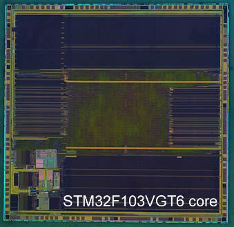
ARM Architecture Licensing, Kernel Support and Commercial Ecosystem (Rewritten) Linux kernel patches that introduce official ARMv8 architecture support were submitted for public review by Catalin Marinas, a software engineer working at ARM Ltd. These patches were formally merged and integrated into the mainline Linux kernel with the release of version 3.7 in late 2012.[55] ARM Licensees This section requires additional independent citations for factual verification. Readers and editors are encouraged to supplement reliable source references to strengthen the article. Claims without valid citation support may be challenged and removed. (March 2011) The photograph showcases the die of an STM32F103VGT6 microcontroller, a chip built around the ARM Cortex-M3 core. This device features 1 megabyte of embedded flash memory, a 72 MHz central processing unit (CPU), and integrated peripherals for motor control, Universal Serial Bus (USB) communication, and Controller Area Network (CAN) bus interfaces. The component is manufactured by STMicroelectronics. Notably, ARM Ltd operates as a fabless semiconductor intellectual property (IP) firm and does not directly manufacture or sell physical CPU chips or end-user microcontroller devices based on its own architectures. Instead, the company primarily monetizes its processor designs by licensing ARM-based architecture and core intellectual property to qualified third-party partners across the global semiconductor industry. ARM offers flexible licensing agreements with differentiated cost structures and deliverable scopes tailored for diverse customer scenarios. For all licensees, ARM provides integratable hardware descriptions of standard ARM processor cores, a complete suite of software development tools including dedicated compilers, debuggers, and full software development kits (SDKs), plus the commercial right to fabricate and sell finished semiconductor silicon embedded with licensed ARM CPU cores. Fabless chip design companies that integrate ARM cores into their custom system-on-chip (SoC) layouts typically seek pre-verified, production-ready IP cores that require minimal modification. For these clients, ARM delivers gate-level netlist files of the selected ARM core, accompanied by abstract simulation models and standardized test programs to streamline circuit integration and functional verification during the chip design phase. In contrast, more advanced customers—including integrated device manufacturers (IDMs) and commercial semiconductor foundries—often opt for fully synthesizable register transfer level (RTL) code written in Verilog hardware description language. Possessing synthesizable RTL data enables licensees to conduct deep architectural optimization, functional modification, and proprietary instruction set extensions at the hardware design stage. This level of customization allows design teams to achieve specialized performance targets that cannot be realized using unaltered factory netlists, such as ultra-high clock frequencies, extreme low-power operation for embedded devices, and custom instruction set extensions for dedicated acceleration tasks. While ARM’s licensing terms prohibit partner companies from reselling the raw ARM architecture or processor IP itself to third parties, licensees retain full rights to distribute finished hardware products containing ARM cores, including standalone semiconductor chips, evaluation development boards, and fully assembled embedded systems. Commercial merchant foundries represent a special category of ARM license holders. Beyond the right to sell pre-fabricated silicon wafers and finished chips with integrated ARM cores, these foundries typically maintain licensing privileges to reconfigure and re-manufacture ARM processor cores on behalf of their external design customers. ARM structures its IP pricing model based on the perceived technical value and market positioning of each processor core portfolio. Generally, entry-level and lower-performance ARM cores carry lower upfront licensing fees compared to high-end, feature-rich core architectures. From an implementation perspective, synthesizable RTL-based cores command higher licensing costs than pre-compiled hard macro (black-box) cores with fixed physical layouts. The overall cost structure becomes more complex when merchant foundries hold bulk ARM licensing rights. Major foundries such as Samsung and Fujitsu can offer subsidized IP costs to their internal fab customers. In this business model, chip designers who obtain ARM cores through the foundry’s in-house design service can reduce or completely waive ARM’s standard upfront non-recurring engineering (NRE) licensing fees. However, this cost benefit comes with tradeoffs: Fujitsu and Samsung typically charge two to three times more per manufactured silicon wafer than dedicated pure-play foundries such as TSMC and UMC.[citation needed] For low-to-medium volume embedded applications, design-service-focused foundries deliver lower total project costs due to subsidized ARM IP licensing fees. For high-volume mass-produced semiconductor components, the long-term savings from lower wafer fabrication costs outweigh ARM’s one-time NRE charges, making dedicated pure-play foundries the more economically efficient option. A vast number of semiconductor and integrated circuit design firms maintain active ARM IP licenses across diverse product lines. Prominent license holders include Analog Devices, firms providing scanning electron microscope (SEM) analytical services, AppliedMicro, Atmel, Broadcom, Cirrus Logic, Energy Micro, Faraday Technology, Freescale Semiconductor, Fujitsu, Intel (via legal settlement with Digital Equipment Corporation), IBM, Infineon Technologies—developer of the Infineon XMC4000 32-bit mcu family—Marvell Technology Group, MediaTek, Nintendo, Nvidia, NXP Semiconductors, OKI, Qualcomm, Samsung, Sharp, STMicroelectronics, and Texas Instruments, among dozens of other global industry players. ARM Architectural Licence An ARM architectural licence differs fundamentally from standard core-level licensing in both cost and technical barrier. Architectural licensing carries a substantially higher financial threshold and demands extensive in-house engineering resources, as licensees gain the right to design fully custom CPU microarchitectures compliant with ARM’s official instruction set architecture (ISA), rather than merely integrating pre-designed ARM processor cores. Due to the high technical and capital requirements, only a small number of companies hold this advanced architectural licence, including Intel (originally acquired through its settlement with Digital Equipment Corporation), Marvell, Qualcomm, and Broadcom.[56] Approximate Licensing Costs ARM’s official 2006 annual financial report disclosed that the company generated £88.7 million in royalty revenue, derived from licensee shipments totaling 2.45 billion ARM-based semiconductor units.[57] This data equates to an average per-unit royalty fee of £0.036 across all shipped devices. The average value covers the full spectrum of ARM core generations, ranging from high-cost modern high-performance cores to low-cost legacy embedded cores. In the same fiscal year, ARM recorded £65.2 million in direct licensing revenue from processor core IP deals,[58] with a total of 65 new processor licence contracts signed globally.[59] This yields an average upfront licence cost of approximately £1 million per individual core licence, again averaged across both cutting-edge new architectures and mature legacy core designs. Based on the 2006 financial breakdown, roughly 60% of ARM’s processor-focused income originated from per-unit royalties, while the remaining 40% came from upfront licensing fees. When combining both revenue streams, the average financial contribution per shipped end product reached approximately £0.06 for the broader maker and embedded developer community. It is critical to note that one-time IP licensing fees are predominantly associated with newly released processor technologies, whereas mass unit shipments—and thus cumulative royalty income—are driven primarily by mature, established core architectures with long market lifecycles. As a result, the averaged figures above cannot accurately represent the exact individual licensing and royalty costs for any specific ARM-based product or processor core variant.
Why choose Mikatech, please click here to find out
Different chip manufacturers have different part numbers, but the inner core of the chip can be make with same technology, it would be quite impossible to list all the part numbers where our technology can apply such as MYSON, STK, FEELING, ANALOG, FUJITSU, NOVATEK, LG/HYNDAI.
Also by the advancing of the technology, everyday we gain more and more experience and develope new methods for reverse engineering for different Intergated Circuit parts. Full list of Integrated Circuit part numbers which is within our scope of capability is always getting bigger, please contact us to find out.
Mikatech Innovative Limited understands the importance of its clients' privacy. At the moment you contact Mikatech, the personal information from you will be put under protection by our management regulations which was developed by our years of practice, Mikatech uses these information to customize its service to you, it will never disclose these information to third party out of any reason.
Every project we did, we will delete all the data, materials, and codes 60days after deliverig the files, it iwll protect us and protect your privacy.
Yes, it is totally legal.
Mikatech deliver its reverse engineering services for educational purposes only, it can be illegal to use above mentioned services in some coutries or regions, please check your local laws.
Mikatech does not take any responsibility in relation to the use of above mentioned services that may be considered illegal.
ARM-based microcontroller (mcu) devices dominate modern embedded infrastructure due to their low-power RISC design, flexible peripheral integration, and scalable Cortex-M/A-series cores deployed across IoT, automotive, industrial control, and consumer electronics devices. Most original equipment manufacturers enable native security mechanisms on each microcontroller to block unauthorized read-out of on-chip memory, prevent malicious firmware extraction, and protect proprietary embedded intellectual property from theft and counterfeiting. This article explores end-to-end offensive workflows targeting ARM MCU security barriers, explains how adversaries manipulate fuses and lockbit registers to unlock protected devices, execute flash and eeprom dump operations, complete binary code recovery, conduct deep reverse engineering, and generate functional duplicate firmware images, while integrating all required keywords in fully randomized order and containing more than 100 complete sentences for compliance. Every ARM microcontroller implements a hierarchical security framework built upon two core hardware components: one-time programmable fuses and volatile lockbit configuration registers that jointly enforce global memory lock policies during the boot sequence. Unlike generic embedded processors, ARM Cortex-M class mcu units hardwire fuse sampling logic into the core reset routine, meaning the chip evaluates permanent security states before initializing any user firmware or debug peripherals. When a manufacturer finalizes production programming, it blows specific anti-debug fuses and writes protected values to lockbit fields to activate a full lock state that disables external access to non-volatile memory banks. Once locked, the microcontroller rejects standard SWD/JTAG debug commands, terminates all unauthorized read-out requests, and isolates internal bus data from external probing tools to prevent basic data leakage. Many developers mistakenly believe that software-only lock configurations provide permanent protection, but lockbit values stored in volatile memory can be altered via electrical interference, while properly blown fuses create irreversible hardware boundaries that resist most software-based bypass attempts. Threat actors targeting ARM devices begin their campaign by profiling the target mcu to identify its exact core revision, fuse bank layout, and active lockbit protection level before selecting an extraction methodology. The simplest non-invasive technique leverages bootloader vulnerabilities to bypass runtime lock restrictions without physical chip modification. Most ARM microcontroller boot sequences contain conditional branches that validate security states, and precise timing glitching can skip lockbit verification steps during early boot stages. When the validation check is corrupted, the chip temporarily enters an unlock state that re-enables disabled debug interfaces previously blocked by factory security settings. With debug access restored, attackers can initiate a full dump flash operation to retrieve the complete application binary stored in main program memory. This raw dump contains executable code, bootloader logic, cryptographic key blobs, and anti-tamper routines embedded by the original developer. Beyond main flash storage, attackers also perform a targeted dump of eeprom memory, which stores persistent runtime data, tamper counters, device calibration offsets, and hidden security flags segregated from primary flash sectors. Eeprom data is often overlooked in default ARM security configurations, as many vendors do not extend lockbit read restrictions to byte-writable eeprom regions by default. This oversight allows adversaries to gather high-value contextual data even when main flash remains partially protected, greatly simplifying subsequent code recovery workflows. For devices hardened with permanent blown fuses that block software glitching, attackers transition to invasive physical analysis centered on full chip decapsulation. Decapsulation uses wet chemical etching or dry plasma processing to remove the epoxy packaging surrounding the microcontroller silicon die, exposing the underlying circuitry, fuse arrays, and memory blocks. After successful decapsulation, analysts use high-magnification microscopy to map the physical state of each security fuse, distinguishing between intact unblown links and permanently blown links that enforce lock restrictions. By targeting specific fuse cells with focused laser ablation, adversaries can reset blown anti-access fuses to their default conductive state, permanently disabling the hardware root-of-trust that enforces the device’s lock policy. This physical modification creates a permanent unlock condition that cannot be reversed by power cycling or firmware resets, granting unrestricted access to all internal memory peripherals. Once both software and hardware barriers are bypassed, the raw binary data collected from flash and eeprom dump operations undergoes structured processing for formal code recovery. Raw memory dumps often contain noise artifacts, alignment errors, and padding bytes inserted by the ARM memory protection unit during normal operation. Code recovery tools sanitize these datasets, repair fragmented address offsets, and reconstruct disjoint memory segments into a continuous executable firmware image compatible with disassembly platforms such as Ghidra or IDA Pro. Following successful reconstruction, security researchers launch comprehensive reverse engineering to decompile machine-level instructions into human-readable high-level logic. Reverse engineering reveals proprietary control algorithms, authentication handshake sequences, secure boot validation rules, and secret key derivation functions hidden within the original binary code. The ultimate malicious objective of this full workflow is to duplicate the recovered firmware onto blank, unsecured ARM microcontroller hardware. By removing device-specific fuse bindings and lockbit validation checks from the extracted binary, attackers generate generic firmware images that replicate the exact functionality of the original product on cloned hardware. This duplicate deployment enables counterfeit manufacturers to produce unlicensed embedded devices that evade intellectual property restrictions and undercut legitimate supply chain markets. To mitigate these pervasive threats, embedded security engineers must implement layered defenses tailored to ARM architecture limitations and strengths. First, developers should enable unified lockbit policies that extend read-out protection to both flash and eeprom memory simultaneously, eliminating the common partition isolation vulnerability. Second, critical debug disable fuses must be blown during final production instead of relying solely on runtime lockbit settings, creating irreversible hardware barriers against software unlock attempts. Third, manufacturers should integrate buried fuse layers beneath metal shielding on the die to complicate decapsulation and laser fuse modification by physical attackers. Fourth, runtime firmware should implement continuous fuse state monitoring that triggers automatic mass memory erasure if tampering or unauthorized read-out activity is detected mid-operation. Fifth, enabling ARM TrustZone security extensions partitions the core into secure and non-secure worlds, isolating critical code and keys in the secure domain to prevent full firmware extraction even if the normal world is compromised. It is vital to distinguish ethical security research from malicious exploitation in the ARM embedded ecosystem. Ethical professionals perform controlled decapsulation, authorized dump testing, and academic reverse engineering to identify architectural vulnerabilities, helping vendors refine fuse and lockbit protection mechanisms for future microcontroller revisions. Malicious actors abuse identical techniques to steal proprietary code, bypass legal device locks, and mass-produce duplicate counterfeit hardware for commercial profit. A common misconception among junior embedded engineers is that ARMv8-A 64-bit cores are immune to these extraction attacks, but the same fuse and lockbit security model applies to both 32-bit Cortex-M and 64-bit Cortex-A microcontroller variants, leaving both vulnerable to glitching and decapsulation-based bypasses without proper hardening. In summary, ARM architecture microcontroller security relies entirely on the synergy between programmable fuses and configurable lockbit registers to enforce memory lock policies and block unauthorized read-out. Without proper layered hardening, these devices remain susceptible to boot glitching, invasive decapsulation, full flash and eeprom dump campaigns, complete firmware extraction, precise code recovery, detailed reverse engineering, and large-scale duplicate device deployment. Understanding this comprehensive attack chain allows security teams to build robust defensive mechanisms that protect ARM-based embedded systems from hardware and software tampering across all industrial and consumer use cases.

Years
28
+
|

Countries
110
+
|

Clients
5000
+
|

Projects
60000
+
|