Atmel AT91SAM Series Successfully Hacked
Atmel produces a number of ARM based devices in their portfolio of products. We had one laying around the lab so here we go as usual…
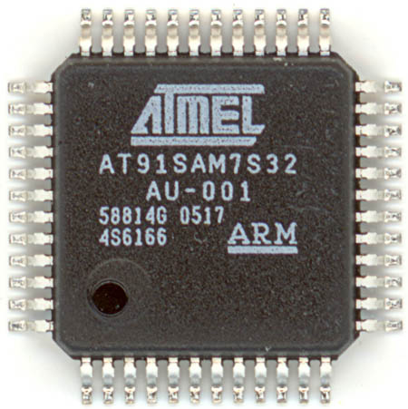
The device was a 48 pin QFP type package. We also purchased a sample of the other members of the family although the initial analysis was done on the AT91SAM7S32 part shown above. All pictures will relate to this specific part even though there is not a signifigant difference between the other members of this line except memory sizes.
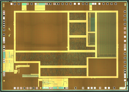
After decapsulating the die from inside the QFP, we find a beautifully layed out 210nm 5 metal design! Thats right, 5 metal layers! Strangely enough fib focused ion beam microscopy, we would have thought this was a 220nm 5 metal but apparently Atmel doesn’t have a .22um process so this is matching their .21um.
The core runs at 1.8v and allows 1.65v operation maker together club (thus it is their ATC20 process being used). The datasheet on the device can be found here. The 32KB Flash part also contains 8KB of SRAM (that’s a lot of ram!).
Notice on this particular layout, there is CMP filler metal (e.g. dead metal, metal slugs that are not connected to anything floating in SIO2) covering almost the entire die.
The picture above actually has had the top 2 metal layers removed. Metal 5 (M5) being the highest with the CMP filler and some power planes. Metal 4 (M4) had additional power planes and routing wires.
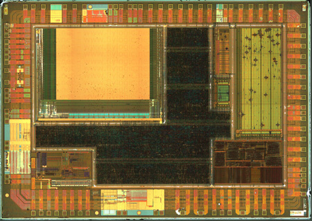
With Metals 1-3 still present, we can get a nice overview of the floorplan now. We can see the Flash, Fuses, and SRAM clearly. The Flash has a solid coating of metal over the entire cell area which has become common from Atmel to prevent UV light attacks we suppose?
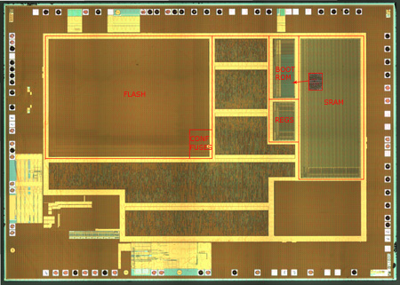
We can now label the areas on the original top metal overview photo. There is a small boot-rom loader present on the device as well and is explained in the manual.
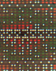
The picture above shows some of the bits of this ROM.
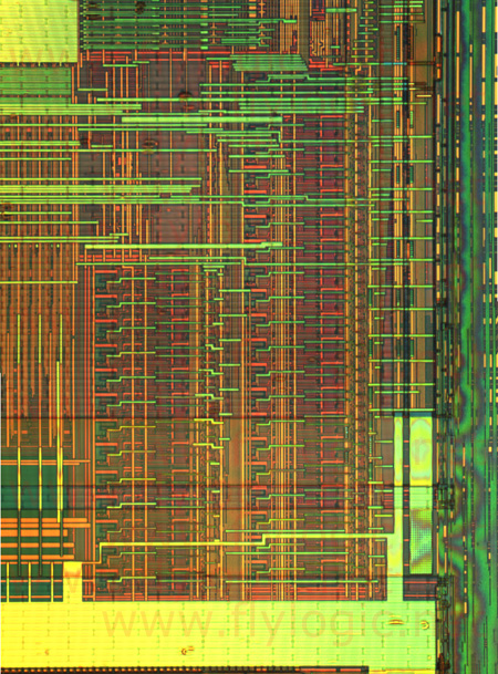
In the above picture lay the configuration fuses. Single cell’s of EEPROM type memory where any given cell can be set or cleared independently of another. Atmel layed them out very orderly as we see typically. It should be noted that these fuses are buried under 3 metal layers!
These cells were actually on Metal 1 and 2 but there are connections via Metal 3 as well.
There were additional power planes across the lower area of the photo from Metal 4 and 5 that cover those fuses however this isn’t buying them any security if the actual lock bits were buried there. A laser can go right through it all keeping the power-bus in tact with a hole in it.
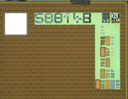
Finally, the Atmel part number of this die. The CMP filler is visible in this picture too.
In summary, this is a very well secured device. firmware recovery Fuses buried in a 5 metal layer design make the Microchip DSPIC’s look like a piece of cake in comparision (They are 350nm 4 metal).
However, by the hard work of our Mikatech Team, below SAM series is now in our service list in june 2009:
AT91SAM9XE512 AT91SAM9XE256 AT91SAM9XE128 AT91SAM7S64B AT91SAM7S32B AT91SAM7SE512 AT91SAM7SE256 AT91SAM7SE32 AT91SAM7XC512 AT91SAM7XC256 AT91SAM7XC128 AT91SAM7X512 AT91SAM7X256 AT91SAM7X128 AT91SAM7S161 AT91SAM7S512 AT91SAM7S256 AT91SAM7S128 AT91SAM7S64 AT91SAM7S321 ...
|